Technological advancements and miniaturization
Decades ago, when people sat down to watch television, the video image beamed through a cathode ray tube where electrons were shot onto a phosphor screen. The TV unit was large, heavy and full of hazardous waste materials. Also, at that time, corporations like banks and retail chains stored data on large, room-sized computer systems. Today, mobile phones provide safer, better resolution images than old television sets. It can hold more data than a 1970s IBM mainframe and a VAX computer of the 1980, and it receives in seconds a night’s worth of video watching.

Diagram of grazing incidence diffraction
Moore’s law, proposed in 1965, predicted that the number of components in an integrated circuit would double yearly, thanks to a number of enabling factors: metal-oxide transistors (MOSFETS), 3D integrated circuits (3D ICs), chemical-mechanical planarization (CMP), and deep UV excimer laser photolithography. Today, memory chips smaller than a postage stamp can hold hundreds of gigabytes of data. This is more data than a room full of IBM mainframes.
Applications of thin film technology
However, doubling integrated circuits is only part of the story. Thin film technology is another important technology driving computing, entertainment, communication and energy collection. Thin films are two-dimensional systems of great importance to many real-world problems. Their material costs are small compared to the corresponding bulk material, and they perform the same function when it comes to surface processes. Thus, knowledge and determination of the nature, functions and new properties of thin films have been used in the development of new technologies and emerging applications.
Further, advances in thin film deposition techniques during the 20th century have enabled a wide range of technological breakthroughs in areas such as magnetic recording media, electronic semiconductor devices, LEDs, optical coatings (such as antireflective coatings), hard coatings on cutting tools, and for both energy generation (solar cells) and storage (batteries). It is also being applied to pharmaceuticals, via thin film drug delivery systems.
Multilayer devices
A stack of thin films is called a multilayer, and many devices are now composed of multilayer devices, likely even the screen you are looking right now. While thin film transistors play a major role in video devices and in computer chips, an emerging application for thin film technology is energy collection, i.e., solar panels. Thin film solar panels have light-absorbing layers about 350 times smaller than that of a standard silicon panel. Because of their narrow design and the efficient semiconductors built into their cells, the panels are extremely lightweight yet still maintaining strong durability. These materials are thin enough to be flexible, allowing them to be deposited on flexible substrates to fit several form factors for storage, transportation and installation.
This blog is part of our “New Materials are Getting Thinner and Thinner” series. In Part 2, we’ll look at how thin film technology is used today.
To learn how thin films can be measured using X-ray diffraction, read our published application note, Investigation of Ni on Si thin film with ARL EQUINOX 100 X-ray Diffractometer.
Want to speak to someone? Need a quote? Want a demo? |
Opt in for email communications on this and other topics. |

FTIR in Specialty Gas Production: From Purity Verification to Process Insights
Introduction Specialty gases are essential to advanced manuf... Olivia Madamba
Read More
Enhancing aircraft engine performance
SEM analysis of René N5, a nickel-based superalloy for hig... Alice Scarpellini
Read More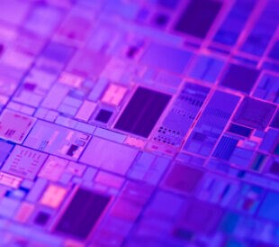
Why Ultra-High-Purity Gas Analysis Outperforms Conventional Methods in Semiconductor Manufacturing
As semiconductor production reaches unprecedented levels of ... Daniel Merriman
Read More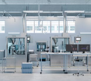
Modular Multiplex Raman vs. Traditional Multiplexing: A Smarter Approach to Process Monitoring
In process analytical technology (PAT), few innovations have... Janam Pandya
Read More
Where’s Part 2?
Hi Carl,
Here is Part 2: https://www.thermofisher.cn/blog/materials/thin-film-applications-in-energy/
Part 3: https://www.thermofisher.cn/blog/materials/fabricating-and-characterizing-thin-film-materials/