Elemental analysis: EELS vs EDS
Secondary signals in electron microscopes allow you to complement high-quality images with high-resolution elemental analysis, identifying the chemical composition of your sample down to individual atoms. In this infographic, we provide an overview of two popular elemental analysis techniques, energy dispersive X-ray spectroscopy (EDS) and electron energy loss spectroscopy (EELS).

What happens in EELS vs EDS?

Comparison of spectra

Images obtained with EELS and EDS

Click here for accessibility descriptions >
Image 1 Title: Elemental Analysis – EELS vs EDS
An illustration depicting the interaction of an electron beam with a thin sample material. The electron beam, which is depicted as a dotted line, hits the surface of the sample. The sample emits ejected sample electrons and transmitted beam electrons through the opposite side, both depicted by dotted lines slightly off angle to the path of the incoming electron beam. Emitted X-rays reflect off the surface of the sample, represented by a wavy line in order to indicate that this is a form of energy.
Captions included on the image:
- Energy dispersive X-ray spectroscopy (EDS, also abbreviated EDX, XEDS, or EDXS) measures the energy of X-rays released from a sample’s surface when it’s irradiated by an electron beam.
- Electron energy-loss spectroscopy (EELS) measures the energy of electrons that pass through the specimen as they inelastically collide with the sample’s electrons.
Image 2 Title: What happens?
This figure is split into two halves, with EELS information on the left and EDS information on the right. An illustration depicting the interaction of a beam electron with a sample atom is shown in both columns, but with different elements emphasized, depending on what is relevant to the technique. The atom is represented by a stylized nucleus surrounded with two concentric rings of electrons. The inner ring has 2 electrons and the outer ring has 6 electrons.
One of the inner ring electrons is struck by a source beam electron and knocked off of the atom, with an empty circle representing its absence. The source beam electron is deflected off of this empty circle and is now labeled as an EELS electron. An electron on the outer ring has an arrow pointing toward the empty circle, indicating that it will fill this vacant position. A wavy line, representing an emitted X-ray, is shown pointing away from the atom as a result of the outer ring electron moving to the inner ring.
Captions included on the image:
- EELS: An electron beam inelastically impacts a sample atom and EELS subsequently detects this electron as it leaves with a reduced energy that depends on the electron shell it interacted with.
- EDS: An electron beam inelastically impacts a sample atom and a core shell electron is knocked off. A higher energy electron fills the hole left behind in order to stabilize the atom. The difference in energy of this electron’s initial and final position is released as an X-ray. EDS detects this X-ray, which has a specific energy characteristic of that electron transition.
Image 3 Title: What does this tell you?
This figure is split into two halves, with EELS information on the left and EDS information on the right.
The left column shows an idealized EELS spectrum, with electron energy loss (in eV) on the x-axis and relative frequency on the y-axis. There is a tall zero loss peak on the far left, followed by a slightly shorter and broader plasmon resonance peak. An inset shows a close up of the right portion of the spectrum. The inset contains the relatively small atom core-loss peak, to its right are smaller peaks that correspond to fine structure information.
The right column shows an EDS spectrum of a mineral sample, with energy (in keV) labeled on the x-axis and no y-axis label. Numerous peaks are individually labeled with the element they correspond to: the most prominent include a carbon peak on the far left followed by an oxygen peak that is approximately twice as tall. On the far right is a prominent iron peak that is slightly shorter than the oxygen peak.
Both images are attributed to Wikimedia Commons user Hat’nCoat under Creative Commons BY 3.0.
Captions included on the image:
- EELS: The low-energy peak corresponds to interactions with weakly bound outer shell electrons. The high-energy peak corresponds to collisions with the core shell electrons. The fine details of these two peaks can provide information on the atom of origin and its bonds to its neighbors.
- EDS: The peaks of an EDS spectrum correspond to the unique electron transitions in the atom of origin. The ratios of the peaks give insight into the relative amount of each element in the sample.
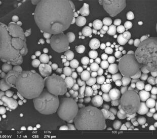
Image 4 Title: Comparison of EELS and EDS
This figure is split into two halves, with EELS information on the left and EDS information on the right.
The left column shows a core-loss EELS atomic-resolution elemental map of a BaTiO₃/SrTiO₃ interface.
The right column shows an SEM image of electroplated bimetallic metal foams colorized with EDS data. Sample courtesy of Prof. Dr. Peter Broekmann, Department of Chemistry and Biochemistry, University of Bern.
Captions included on the image:
- EELS: Suited for light elements and thin samples, as they are less likely to impede the emission of the ejected electron. Provides information on chemical bonding
- EDS: Suited for heavier atoms (higher energy transitions). Suited for thicker samples (signal is reflected off sample, does not need to pass through). Qualitative – quantitative analysis requires comparison to standards.
Related blog posts:
EDX Analysis with SEM: How Does it Work? >>
You Need an Efficient and Intuitive SEM Experience >>
Learn more:
Thermo Scientific ColorSEM Technology enables real-time EDS analysis while imaging >>
EDS analysis >>
EDS elemental analysis >>
EELS analysis >>
//
Alex Ilitchev, PhD, is a Science Writer at Thermo Fisher Scientific.
What is Scanning Electron Microscopy?
How does a scanning electron microscope work? You have likel... Alex Ilitchev, PhD
Read More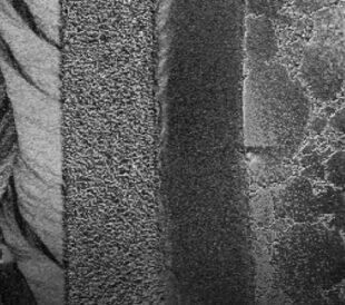
How Does an Electron Microscope Work?
Since the advent of electron microscopy in the 1930s, this r... Alex Ilitchev, PhD
Read More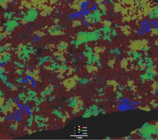
Quantitative EDS mapping of a Monzogabbro Rock Sample
What is rock analysis? Rock analysis provides important info...
Read More
SEM Failure Analysis of Tubular Heating Elements
Tubular heating elements, or Calrod type heaters, are found ...
Read More
Leave a Reply