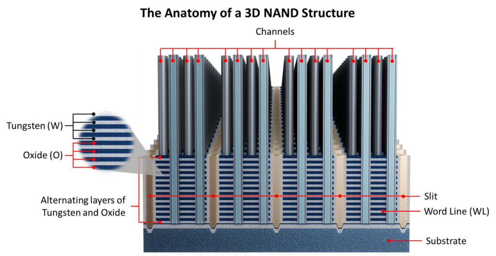
3D NAND flash memory is a type of non-volatile storage that arranges its memory cells in multiple stacked layers instead of spreading them out on a flat surface like older 2D NAND designs. By building upward, it can fit more data into the same area, which increases storage capacity, lowers the cost per bit, and makes it ideal for use in solid-state drives, smartphones, and large-scale data centers. 3D NAND flash memory devices have come a long way over the last half-decade. Five years ago, 2D planar NAND consisted of billions of memory cells densely packed next to each other to provide higher-capacity flash with faster performance. As the ability to pack more cells into sub-1x nanometer planar NAND reached its limits, manufacturers turned to 3D NAND flash memory, a groundbreaking technology stacking memory cells on top of each other in multiple layers to achieve higher capacity, greater reliability, and faster write speeds.
What is the difference between 2D vs 3D NAND flash memory?
Flash memory works by storing data in an array of memory cells made from floating-gate transistors. Each cell can hold one or more bits of information, which is retained even when the power is turned off. The revolutionary process introduced a chemical vapor deposition (CVD) process to stack thin film layers connected with precise holes etched through the entire vertical structure. The first 3D NAND flash memory started shipping in 2013 with 24 layers. 3D NAND flash memory, an advanced form of NAND flash, stacks memory cells vertically in multiple layers to increase storage density and capacity. Through the years, the need to increase capacity to meet data storage demands pushed manufacturers to higher aspect ratios with 3D NAND flash memory advancing to 64, 96, 128, 144 and most recently, 176 layers.
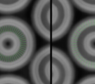
As layers of memory cells have been added, increasing performance, storage capacity, and energy efficiency, the complexity of the fabrication process has also increased. Precise deposition and etching processes have become more challenging, resulting in longer manufacturing times and buried defects in word lines and control gates. Moreover, errors introduced into the fabrication process, such as non-uniform layer thickness or incomplete, bowed, or twisted etched holes, can result in lower yield per wafer and higher costs per terabyte.
Where is 3D NAND flash memory used?
3D NAND is widely used in various applications, including solid-state drives (SSDs), smartphones, tablets, and other mobile devices. It is also utilized in data centers and enterprise storage solutions due to its high capacity and reliability.
What are the key benefits of 3D NAND flash memory?
3D NAND offers several key benefits: higher storage density by stacking memory cells vertically, significantly increasing storage capacity without increasing the physical footprint; improved performance with faster read and write speeds compared to traditional 2D NAND; enhanced endurance with more write cycles, improving the lifespan of the memory; lower power consumption, making it ideal for mobile devices and data centers where power efficiency is crucial; and cost-effectiveness due to increased storage density and improved manufacturing processes.
Where does 3D NAND flash memory analysis take place?
Today, many 3D NAND manufacturers send samples to labs for analysis. Between transit time, waiting for the lab to process the sample, and receiving the results, the fab can be delayed for days or even weeks. This leads to longer development cycles, increased manufacturing cost, slower time-to-market, and reduced profits. But what if there were a better way for the fab to more quickly get the data and insights they need to improve and maximize their processes?
How can defects be identified in 3D NAND flash memory?
As 3D NAND layer counts increase, it’s increasingly difficult to identify defects in these complex high-aspect ratio structures, slowing development cycles and increasing cost-per-bit. An inline, easy-to-use system that combines high-resolution, high-contrast imaging with automated delayering and milling would allow busy fabrication customers to obtain unprecedented insights into the entire stack of their high-aspect-ratio structures, right within the fab. This would significantly reduce time-to-data, accelerate process and device development, and bring innovative products to market more quickly.
Learn how the new Thermo Scientific Helios 5 PXL PFIB Wafer DualBeam reduces time-to-data for through-stack metrology of advanced 3D structures from days to hours.

Written in collaboration with Sean Zumwalt, Senior Marketing Manager for semiconductors at Thermo Fisher Scientific.
Enhancing High-Volume DRAM Manufacturing with Automated TEM Metrology and Characterization
Dynamic random-access memory (DRAM) plays a crucial role in ... Dr. Zhenxin Zhong
Read More
Faster time to data in the fab with multi-ion species plasma FIB
This quarter, I am excited to share the news about a newly r...
Read MoreHigh-Quality TEM Lamella Preparation: Critical Factors and Best Practices
Introduction: The quality of transmission electron microscop... Abhi Barve
Read More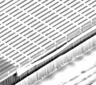
Removing Large Volumes of Material Fast with FIB-SEMs
Focused ion beam scanning electron microscopes (FIB-SEMs) ar...
Read More
Leave a Reply