This quarter, I am excited to share the news about a newly r...
Read More Faster time to data in the fab with multi-ion species plasma FIB
Semiconductor manufacturing stories and solutions about a more connected, more autonomous, and smarter world
This quarter, I am excited to share the news about a newly r...
Read More Faster time to data in the fab with multi-ion species plasma FIBIntroduction: The quality of transmission electron microscop... Abhi Barve
Read More High-Quality TEM Lamella Preparation: Critical Factors and Best Practices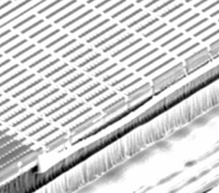
Focused ion beam scanning electron microscopes (FIB-SEMs) ar...
Read More Removing Large Volumes of Material Fast with FIB-SEMs
What is the current state of TEM in semiconductor analysis? ... Dominique Delille
Read More Transmission Electron Microscopy in Semiconductors: Generating Ground Truth Insights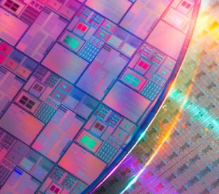
Semiconductor fabrication challenges Semiconductor fabricati... Abhi Barve
Read More Accelerating Semiconductor Device Analysis with the Power of the Helios 5 EXL Wafer DualBeam
Automated metrology for high-volume semiconductor manufactur... Dr. Zhenxin Zhong
Read More Automated Metrology Becomes a Reality with New Scanning Transmission Electron Microscope
3D semiconductor packaging industry insights from Semicon Ko...
Read More Unraveling 3D Semiconductor Packaging ChallengesFocused ion beam scanning electron microscopes for precision... Abhi Barve
Read More Nanoscale Microscopy with Gallium FIB SEMStaying ahead of an evolving semiconductor landscape Since 2... Abhi Barve
Read More Chip Complexity and Global Semiconductor Talent Needs Drive Demand for Automation in Semiconductor Manufacturing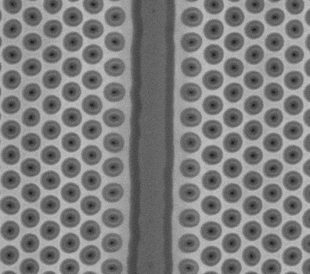
Advanced metrology for 3D NAND structure manufacturing In th... Mark Najarian
Read More How Advanced Metrology Workflows Solve Critical 3D NAND Structure Challenges