The first three blogs in this series focused on present-day challenges in mainstream display technology. In this fourth and final post, we’ll look at next-generation technologies, the measurement challenges they present in R&D and materials engineering, and solutions via thin film encapsulation, new quantum dot technology, and more.
Creating better display technology
Today, the mainstream is populated with liquid-crystal display (LCD) and organic light-emitting diode (OLED) technologies, with many applications transitioning from LCD to OLED. To compete with OLED, many LCD manufacturers are developing technologies such as quantum-dot LED (QLED) and mini-LED.
The industry is investing in areas such as active-matrix OLED, micro-OLED, and next-generation quantum dots (e.g., pixel-color conversion QDs), as well as micro-LED display technology and electroluminescent quantum dots—both of which demand extreme precision in design and production.
Thin film encapsulation to protect OLED devices
Because organic materials are susceptible to environmental degradation, innovation is occurring in thin film encapsulation to protect OLED devices. Thin film encapsulation will extend device lifetime and expand the range of possible applications via new form factors.
As an example, a suitable film can be created by laminating materials such as alumina (Al2O3) and zirconia (ZrO2) in alternating layers. It is crucial to control the thickness of every layer and identify the phase at each interface, and both tasks are accomplished more easily with data from a transmission electron microscope (TEM). When implemented correctly, the interfaces enable the hermetic properties of OLED thin-film encapsulation, preventing the diffusion of oxygen and moisture into the OLED (Figure 1).
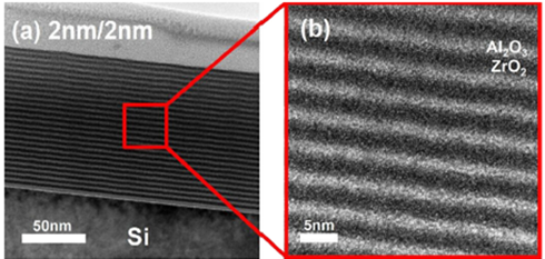
Figure 1. TEM can image alternating oxide layers, each of which is about 2 nm thick. Image from dx.doi.org/10.1016/j.tsf.2015.12.044
Assessing these layers requires a workflow that uses a dual-beam for sample preparation and a TEM for imaging. In addition, high-efficiency X-ray energy dispersive spectroscopy (XEDS) provides chemical information about the layers. Thermo Fisher Scientific provides an industry-benchmark workflow based on the Thermo Scientific Helios 5 Small DualBeam and Talos F200E TEM. From sample preparation to imaging, this approach provides remarkable quality with the shortest time to data.
Actualizing nano-encapsulation of quantum dots
Developers of quantum dot technology are pursuing three major goals: engineering new types of quantum dots that improve image quality; exploring environmentally friendly materials; and developing technologies that actualize nano-encapsulation of nanoparticles.
Semiconductor quantum dots range from to 2 to 10 nanometers, and the size determines the emitted color. Thus, particle size and distribution are critical success factors. For measurements and characterization, TEM is a powerful tool in the process-control stage and in R&D during the formulation and engineering of nanoparticles (Figure 2).
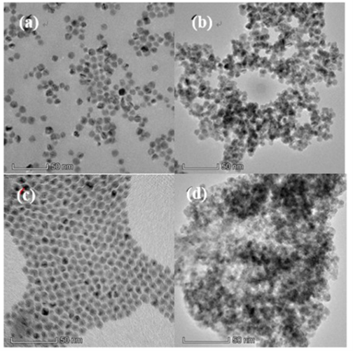
Figure 2. Analyzing particle size and distribution is essential to the advancement of quantum dot displays. Image from SID 2019 Digest, pages 30-33.
It’s also important to understand the core/shell structure of nanoparticles (Figure 3). However, some quantum dots are beam-sensitive and extended exposure can damage QD materials. In such cases, the most effective approach uses fast, low-dosage measurements that extract the most information in the least time.
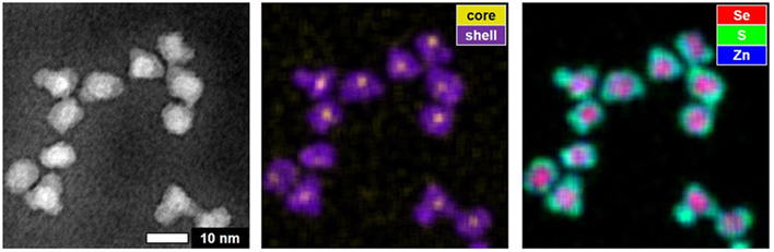
Figure 3. Low-kV scanning/transmission electron microscopy ((S)TEM) enhances microstructural imaging of particles and, ultimately, the implementation of nano-encapsulation technology. Image from doi.org/10.1038/s42256-020-00289-5.
To meet this need, the Thermo Scientific Spectra Ultra (S)TEM offers the highest efficiency among commercially available energy dispersive spectroscopy (EDS) solutions. This enables stable operation under a low accelerating voltage, minimizing damage to beam-sensitive materials and supporting the use of analytical techniques such as EDS mapping or thermography over extended periods.
Enhancing the quantum efficiency of micro-LED display technology
The manufacturing of micro-LED display technology presents many challenges, and recent literature has described a workflow that improves the analysis process. In typical practice, plasma etching will damage multiple quantum-well structures, and this creates larger leakage currents that reduce the quantum efficiency of the device. A dual-beam is used for sample preparation at different locations, or perhaps for different crystal orientations, and then a TEM is used to better understand the full extent of the damage.
Enabling new form factors with thin film encapsulation
Form factor continues to be a driving force in the display marketplace. Consequently, substantial amounts of time and money are being invested in the pursuit of innovative backplane materials.
Here, a TEM workflow is especially useful. One example is the application of oxide thin-film transistors to a flexible backplane. This requires incorporation of polytetrafluoroethylene material into the oxide thin-film transistors to form the amorphous phase and enhance stiffness. To ensure the desired properties, a TEM can be used to identify, at nanometer scale, the phase of the resulting layer. In such cases, the Helios 5 Small DualBeam can be used to prepare samples for visualization using the Talos F200E TEM.
Addressing current and evolving needs
This four-part series on display technology touched on present and emerging topics of interest in the semiconductor industry. Across those topics, Thermo Fisher offers industry-leading solutions that address crucial challenges in three key areas: process metrology, failure analysis, and R&D. Whether your focus is on optimizing mainstream technologies or pursuing pathfinding developments, we offer solutions that support accurate fault isolation, detailed imaging, precise metrology, and advanced analysis.

//
Xiaoting Gu is a product marketing manager at Thermo Fisher Scientific
Enhancing High-Volume DRAM Manufacturing with Automated TEM Metrology and Characterization
Dynamic random-access memory (DRAM) plays a crucial role in ... Dr. Zhenxin Zhong
Read More
Faster time to data in the fab with multi-ion species plasma FIB
This quarter, I am excited to share the news about a newly r...
Read MoreHigh-Quality TEM Lamella Preparation: Critical Factors and Best Practices
Introduction: The quality of transmission electron microscop... Abhi Barve
Read More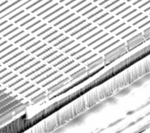
Removing Large Volumes of Material Fast with FIB-SEMs
Focused ion beam scanning electron microscopes (FIB-SEMs) ar...
Read More
Leave a Reply