Hafnium oxide is a highly insoluble thermally stable Hafnium source suitable for glass, optic and ceramic applications. Hafnium oxide is an inert, off-white powder also known as hafnia with a high melting point, it is among the most common and stable hafnium compounds. It is now used as a gate dielectric in semiconductor transistors.

Looking at High-K Thin Film Depositions With Multiple Surface Analysis Techniques
Dielectric materials are not conductive to electricity and are therefore found in semiconductor devices. A commonly used material for gate dielectrics is silicon dioxide (SiO2). However as the thickness of silicon dioxide (SiO2) as the gate material becomes very thin (less than 1.5 nm), the tunnel current increases significantly. Therefore, the need exists for a dielectric material with high K (K is the dielectric constant of the material), which will provide the required electrical properties.
As the devices have continued to shrink, in part enabled by gate oxides grown with atomic layer depositions, new limitations on the bulk Si crystal have forced the industry to look for other alternatives to the traditional transistor concept including the Fin field effect transistor (FinFET) that Intel introduced into production with the 22 nm node. The gate oxide for these advanced devices are often extremely thin, high-k dielectrics, like Hafnium Oxide (HfO2).
In this design, the fins need to be covered with a gate oxide of great compositional and thickness uniformity and without pinholes, a task tailored for ALD. Measurement of the gate oxides’ compositional and thickness uniformity, and the appearance of pinholes, is of critical importance to assuring confidence in the process, as well as understanding factors which affect yield. A multi-technique surface analysis using a fully-automated instrument provides the capability to measure the composition, coverage and band gap analysis of ALD-grown ultra thin films.
In the example described, the high-k dieletric thin film HfO2 is deposited onto a silicon oxide on silicon wafer (SiO2/Si) via ALD. After each ALD cycle, the thickness of deposited HfO2 is quantified over the length of the ALD process by extracting thickness information from XPS data. XPS is firstly used to quantify the amount of hafnium deposited onto the substrate and measure the thickness of the HfO2 and SiO2 layers.
In practice, thin film coverage may not be completely uniform during deposition. Quality control in this aspect of sample production though measurements of sample coverage by ISS. In contrast to XPS, ISS extracts spectral information from the top monolayer of the sample only. Using that information, any Si signal acquired in the ion scattering spectroscopy(ISS) spectra indicated and incomplete surface coverage of HfO2. In this example, after 50 cycles the Si peak has been removed from the spectra completely, therefore it can be deduced that the ALD process reaches full coverage between 20 and 50 cycles. Technical details regarding the physics behind this approach is detailed in the app note.
One of the key properties of gate dielectric components or high-k dielectric materials in general is the band gap. This property, denoting the energy difference between the valence and conduction bands of a material, is the driving force behind many desirable material applications, like LEDs, photovoltaics or solar cells.
While band gap measurements can be routinely performed using XPS on most materials, when it comes to high-k dielectric materials, like HfO2, overlap of XPS peaks in the band gap energy region make measurements more difficult. In this example, the all-in-one system includes reflected electron energy loss spectroscopy (REELS) and software that can automatically calculation the band gap of the sample material. Using the same dual source flood gun that is used for charge compensation, the band gap information is obtained, without the need for a second electron source.

Looking at High-K Thin Film Depositions With Multiple Surface Analysis Techniques
Read more about how compositional and thickness information taken from XPS data provides coverage analysis via ISS and band gap measurements via REELS, producing a complete picture of properties vital to the development of ultra-thin film materials for semiconductor applications.

Revolutionizing Aerospace and Defense with Electron Microscopy and Surface Analysis of Passivated Stainless Steel Landing Gear
The aerospace and defense industry is constantly evolving, d...
Read More
Advancing XPS Depth Profiling with the Hypulse Surface Analysis System
Expanding the capabilities of XPS surface analysis As materi... Tim Nunney
Read More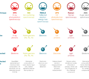
Combining X-ray Photoelectron Spectroscopy with Multiple Surface Analysis Techniques
Updated on Nov. 17, 2021 to reflect the launch of ESCALAB QX... Tim Nunney
Read More
Industrial Uses Of Catalysts
Catalysts in industry Catalysts play a critical role in mode... Carl D. Millholland
Read More
Leave a Reply