Key highlights Compared to conventional package designs, sem... Dr. Adam Stokes
Read More Non-Destructive Semiconductor Defect Detection in Advanced Packaging Technology
Semiconductor manufacturing stories and solutions about a more connected, more autonomous, and smarter world
Key highlights Compared to conventional package designs, sem... Dr. Adam Stokes
Read More Non-Destructive Semiconductor Defect Detection in Advanced Packaging Technology
Artificial intelligence (AI) is reshaping semiconductor desi... Dr. Adam Stokes
Read More Advanced Packaging Failure Mechanisms in the AI Era: Why Reliability Is Shifting in 2.5D and 3D Designs
Dynamic random-access memory (DRAM) plays a crucial role in ... Dr. Zhenxin Zhong
Read More Enhancing High-Volume DRAM Manufacturing with Automated TEM Metrology and Characterization
This quarter, I am excited to share the news about a newly r...
Read More Faster time to data in the fab with multi-ion species plasma FIBIntroduction: The quality of transmission electron microscop... Abhi Barve
Read More High-Quality TEM Lamella Preparation: Critical Factors and Best Practices
Focused ion beam scanning electron microscopes (FIB-SEMs) ar...
Read More Removing Large Volumes of Material Fast with FIB-SEMs
What is the current state of TEM in semiconductor analysis? ... Dominique Delille
Read More Transmission Electron Microscopy in Semiconductors: Generating Ground Truth Insights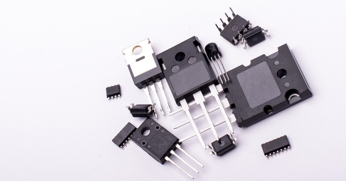
World energy consumption is expected to grow by nearly 50% b... Dr. Adam Stokes
Read More Physical and Electrical Failure Analysis of Power Semiconductor Devices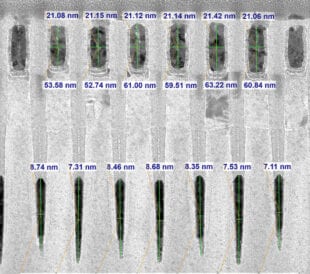
As I discussed in my 2024 year-end article, the semiconducto...
Read More Revolutionizing the way TEM metrology data is collectedGrowing need for semiconductor nanoprobing As the semiconduc... Dr. Adam Stokes
Read More Semiconductor Nanoprobing Boosts TEM Analysis Success Rates on Advanced Logic Devices