Key highlights Compared to conventional package designs, sem... Dr. Adam Stokes
Read More Non-Destructive Semiconductor Defect Detection in Advanced Packaging Technology
Semiconductor manufacturing stories and solutions about a more connected, more autonomous, and smarter world
Key highlights Compared to conventional package designs, sem... Dr. Adam Stokes
Read More Non-Destructive Semiconductor Defect Detection in Advanced Packaging Technology
Artificial intelligence (AI) is reshaping semiconductor desi... Dr. Adam Stokes
Read More Advanced Packaging Failure Mechanisms in the AI Era: Why Reliability Is Shifting in 2.5D and 3D Designs
Dynamic random-access memory (DRAM) plays a crucial role in ... Dr. Zhenxin Zhong
Read More Enhancing High-Volume DRAM Manufacturing with Automated TEM Metrology and Characterization
World energy consumption is expected to grow by nearly 50% b... Dr. Adam Stokes
Read More Physical and Electrical Failure Analysis of Power Semiconductor Devices
Semiconductor fabrication challenges Semiconductor fabricati... Abhi Barve
Read More Accelerating Semiconductor Device Analysis with the Power of the Helios 5 EXL Wafer DualBeamOur everyday lives are changing at a rapid pace. The evoluti... Dr. Adam Stokes
Read More Failure Analysis of Wide Bandgap (WBG) Semiconductor Devices: Techniques and Root-Cause Insights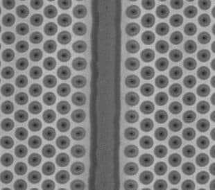
Advanced metrology for 3D NAND structure manufacturing In th... Mark Najarian
Read More How Advanced Metrology Workflows Solve Critical 3D NAND Structure Challenges
Advanced semiconductor packaging calls for advanced failure ... Dr. Adam Stokes
Read More New Ablation Solution for Advanced Semiconductor Packaging Increases Helios PFIB Throughput and Precision
Seeking enhanced performance with compound semiconductor waf...
Read More Using Electron Channeling Contrast Imaging to Optimize Defect Analysis and Wafer Fabrication
For decades, the semiconductor industry has been defined by ... Dr. Adam Stokes
Read More Advanced Semiconductor Packaging: Bringing Stacked Chips Together