
Scanning electron microscopes (SEMs) have become powerful and versatile tools for material characterization, especially in recent years, as the size of materials used in various applications continues to shrink.
Electron microscopes use electrons for imaging in a similar way that light microscopes use visible light. Unlike transmission electron microscopes (TEMs), which detect electrons that pass through a very thin specimen, SEMs use the electrons that are reflected or knocked off the near-surface region of a sample to create an image. Since the wavelength of electrons is much smaller than that of light, the resolution of SEMs is superior to that of a light microscope.
How does scanning electron microscopy work?
In scanning electron microscopy, the electron beam scans the sample in a raster pattern. First, electrons are generated at the top of the column by the electron source. These are emitted when their thermal energy overcomes the work function of the source material. They are then accelerated and attracted by the positively-charged anode.
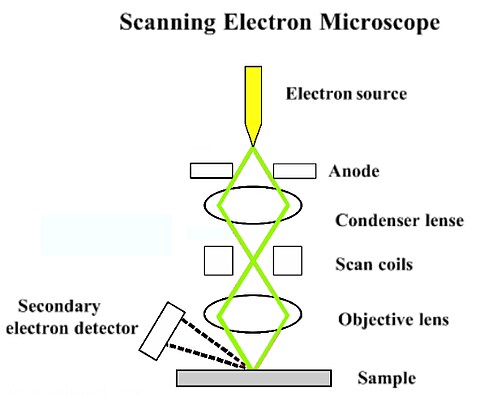
Electrons originate from the electron source before being controlled by an anode, condenser lens, scan coils, and objective lens. The electrons then interact with the sample and are collected and interpreted by a secondary electron detector.
The entire electron column needs to be under vacuum. Like all components of an electron microscope, the electron source is sealed inside a special chamber to preserve vacuum and protect it against contamination, vibrations, and noise. In addition to protecting the electron source from being contaminated, vacuum also allows the user to acquire a high-resolution image. In the absence of a vacuum, other atoms and molecules can be present in the column, which would interact with and deflect electrons, reducing the image quality. High vacuum also helps the detectors in the column collect electrons more efficiently.
SEM instrument components and principles explained
Similar to optical microscopes, electron microscopes use lenses to control the path of the electrons. However, they use electromagnetic lenses because electrons cannot pass through glass. These lenses consist of coils of wire inside metal pole pieces. When current passes through the coils, a magnetic field is generated. As electrons are very sensitive to magnetic fields, their path inside the microscope column can be controlled by these electromagnetic lenses simply by adjusting the current that is applied to them.
Generally, two types of electromagnetic lenses are used: a condenser lens and an objective lens. The condenser lens converges the electron beam, which opens again and is converged once more by the objective lens before hitting the sample. The condenser lens defines the size of the electron beam (which defines the resolution), while the objective lens focuses the beam onto the sample.
The SEM’s lens system also contains scanning coils, which are used to raster the beam onto the sample. In many cases, apertures are combined with the lenses to control the size of the beam.
Secondary vs backscattered electron detection in SEM
The interaction of electrons within a sample can generate many different types of electrons, photons, or irradiations. In the case of an SEM, the two types of electrons used for imaging are backscattered (BSE) and secondary electrons (SE).
BSEs belong to the primary electron beam and are reflected after elastic interactions between the beam and the sample. In contrast, secondary electrons originate from the atoms of the sample. They are a result of inelastic interactions between the electron beam and the sample.
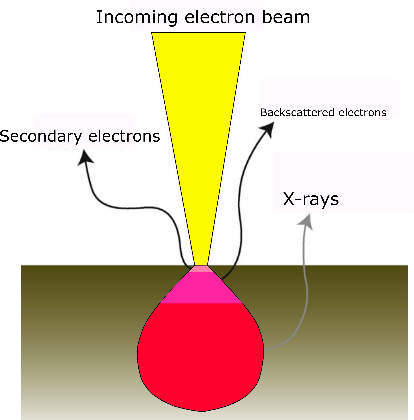
Secondary electrons come from the surface of a sample, backscattered electrons penetrate into the sample, and X-rays come from farther into the sample.
Because BSEs come from deeper regions of the sample whereas SEs originate from surface regions, the two carry different types of information. BSE images show high sensitivity to differences in atomic number; the higher the atomic number, the brighter the material appears in the image. SE imaging can provide more detailed surface information.
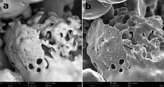
In the BSE image, elements with a higher atomic number are brighter. The SE image provides a clearer view of surface topography.
In many microscopes, detection of X-rays generated from the electron-matter interaction is also widely used to perform elemental analysis of the sample. Every material produces X-rays that have a specific energy; X-rays are the material’s fingerprint. By detecting the energies of X-rays that come out of a sample with an unknown composition, it’s possible to identify all the different elements that the sample contains.
How are electrons detected in scanning electron microscopy?
BSEs and SEs are detected by different types of detectors. For the detection of BSEs, solid state detectors are placed above the sample, concentrically to the electron beam, to maximize BSE collection.
For the detection of SEs, the Everhart-Thornley detector is mainly used. It consists of a scintillator inside a Faraday cage, which is positively charged and attracts the SEs. The scintillator is then used to accelerate the electrons and convert them into light before reaching a photomultiplier for amplification. The SE detector is placed at an angle at the side of the electron to increase the efficiency of detecting SEs, which are then used to form a 3D-image of the sample shown on a PC monitor.
SEM: magic but meticulous
As you can see, there are different processes that the electrons must go through before an image can be shown on your monitor. Of course, you don’t have to wait for the electrons to finish their journey; the whole process is almost instantaneous, in the range of nanoseconds. At the same time, every “step” of an electron inside the column needs to be pre-calculated and controlled with precision in order to obtain a high-quality image.
The image on the left shows a wider view, while the image on the right provides a more detailed look.
The technology behind scanning electron microscopes is continually being improved, and new applications are still arising, making SEMs fascinating instruments with lots of undiscovered capabilities.
To learn more about the best SEM for your research needs, speak with an expert.
Antonis Nanakoudis is an application and product development specialist for the Phenom Desktop SEM family of products at Thermo Fisher Scientific.

Lightweight Composite Materials for Aerospace Applications: Strength, Compliance, and Precision Analysis
How multi-scale materials characterization supports safer, l...
Read More
The Essential Guide to Raman Microscopy
What is Raman spectroscopy? With Raman spectroscopy, researc...
Read More
Particle Analysis for Micro Machining
With the need for small, precisely crafted parts in products...
Read More
You Need an Efficient and Intuitive SEM Experience
Researchers at today’s industrial labs typically work unde...
Read More
excellent
Well narrated explanation