Focused ion beam scanning electron microscopes for precision defect analysis
Focused ion beam scanning electron microscopes (FIB-SEMs) are essential for precision defect analysis in semiconductor devices. They allow for the removal of thin layers of material at nanometer scale, facilitating structural analysis, failure analysis, and metrology.
Introduced approximately 30 years ago, the Ga+ FIB-SEM combines a gallium focused ion beam and a scanning electron microscope in one instrument. It supports various applications including SEM imaging, cross-sectioning, defect analysis, in situ sample preparation, 3D reconstruction, atom probe tomography preparation, and lamella preparation.
The Ga+ FIB-SEM aids in detecting sub-nanometer defects
When analyzing sub-nanometer defects in semiconductor dies, precise location is often unknown. A Ga+ FIB-SEM, such as the Thermo Scientific Helios 5 DualBeam, enables repeated thinning and imaging of the sample until the defect is located. This technology is preferred for its superior performance and application flexibility.
Why precise FIB energy control is important for nanoscale microscopy
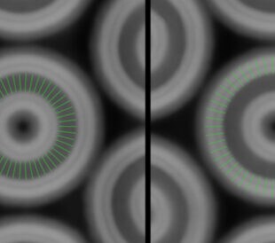
Modern semiconductors include complex structures with hard and soft materials, some of which are beam-sensitive. The ion beam energy determines penetration depth and material removal. High beam energy can damage the region of interest, causing it to become amorphous, while low beam energy may not remove sufficient amounts of material or produce necessary imaging contrast. Therefore, a Ga+ FIB-SEM must support a range of beam energies for different applications.

Comparison of FIB-induced amorphous damage at various voltages (5 kV, 2 kV, 1 kV, and 500 V).
Critical role of high-resolution SEM in semiconductor analysis
SEM resolution is crucial due to the shrinking size of semiconductor features and defects, now often just a few nanometers. High-resolution SEM imaging, especially at low accelerating voltages (<1 kV), is essential for analyzing beam-sensitive materials without causing damage. Automated SEM calibration and alignment ensure consistent imaging performance across different systems and samples. Imaging at low voltages, 2 kV and below, enables the SEM information to come from the surface versus having a mixed signal from deeper in the cross-section face. This supports accurate endpointing on today’s most challenging devices.

Image resolution comparison of a specimen at different voltages (1 kV, 500 V, and 200 V).
Importance of exact navigation and endpointing in semiconductor analysis
Precise navigation to the region of interest (ROI) and exact endpointing are critical for capturing specific features in advanced semiconductor nodes. Endpointing ensures the material removal process stops precisely at the desired location, which is crucial for subsequent TEM analysis.

Accurate endpointing isolates the feature of interest, avoiding projection effects.
Why focused ion beam consistency is necessary for nanoscale microscopy
Spot size consistency and repeatability of the FIB beam affect the resolution, precision, and accuracy of the FIB process. Smaller beam sizes provide higher resolution for removing ultra-thin layers, while larger beams remove material faster but with lower resolution. Maintaining consistency across different samples is challenging but essential. Thermo Scientific DualBeam instruments handle various accelerating voltages, supporting alignment and beam consistency.
How Thermo Scientific instruments address semiconductor analysis challenges
Ga+ FIB-SEMs are vital for nanoscale sample preparation, imaging, and analysis in semiconductor applications. They offer precise beam energy control, high-resolution imaging, advanced navigation and endpointing, and spot size consistency. The Thermo Scientific Helios 6 HD FIB-SEM and the Helios 5 DualBeam family, including the Helios 5 FX, UX, and CX models, provide exceptional capabilities for these tasks.
-
- Thermo Scientific Helios 5 FX
-
- Thermo Scientific Helios 5 UX
-
- Thermo Scientific Helios 5 CX

Enhancing High-Volume DRAM Manufacturing with Automated TEM Metrology and Characterization
Dynamic random-access memory (DRAM) plays a crucial role in ... Dr. Zhenxin Zhong
Read More
Faster time to data in the fab with multi-ion species plasma FIB
This quarter, I am excited to share the news about a newly r...
Read MoreHigh-Quality TEM Lamella Preparation: Critical Factors and Best Practices
Introduction: The quality of transmission electron microscop... Abhi Barve
Read More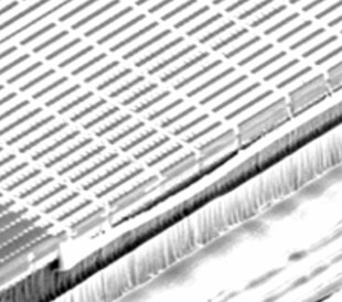
Removing Large Volumes of Material Fast with FIB-SEMs
Focused ion beam scanning electron microscopes (FIB-SEMs) ar...
Read More
Leave a Reply