Process metrology and the development of display technology
Developers of display technology face a host of opportunities and challenges. Opportunities exist across the growing range of screens we view all day, every day. Challenges arise in the pursuit of ever-better picture quality.
Achieving next-generation performance demands innovation in areas such as backplane technology and light-conversion efficiency. The nature of these innovations places a greater dependency on reliable and accurate measurements from process metrology tools.
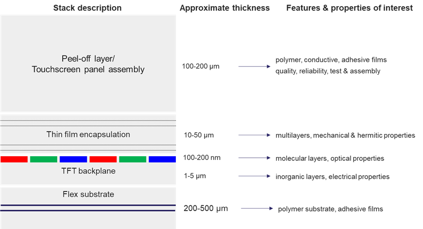
Within a typical display stack, process metrology often focuses on two parts: thin-film transistor (TFT) backplanes and light-emitting units (red, green and blue elements; Figure 1).

Figure 1: The display stack in a mobile device illustrates the layers of interest that affect yield, quality and performance.
In an organic LED (OLED) display, the light-emitting units reside within the thin-film transistor backplane and are comprised of molecular layers 100 to 200 nanometers thick. In this core display technology, optical properties are the key area of interest. The surrounding thin-film transistor backplane contains inorganic layers totaling 1 to 5 microns thick. Crucial failures occur here, and electrical properties are of primary interest.
Imaging the thin-film transistor backplane
As display resolution increases, features get smaller and structures become more complex. Consequently, it is increasingly important to control both the lateral and vertical critical dimensions. Here, process metrology relies on reliable and repeatable measurements.
Measuring lateral critical dimensions depends on the resolution of the imaging tool. A versatile solution such as the Thermo Scientific Apreo 2 SEM also provides imaging modes that highlight surface features under different contrast settings.
Measuring vertical critical dimensions is more challenging because backplane manufacturing involves thin-film deposition at the atomic level. Traditionally, such measurements have required a cross-sectional workflow: cleave the sample, perform chemical etching of the cross-section, and then view with an SEM.
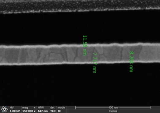
Thermo Fisher Scientific offers the industry’s benchmark workflow based on dual-beam technology: perform a site-specific cut, apply a fine polish with a focused ion beam (FIB), and view the cross-section using high-resolution SEM (Figure 2). The system is also equipped with an automated process metrology solution that ensures the highest repeatability in measurements.

Figure 2. The Thermo Scientific Helios 5 DualBeam can resolve individual layers of a TFT backplane and measure the thickness of each.
Resolving the organic layers with process metrology
Process metrology is more challenging in light-emitting units that have features and layers at nanometer scale. Organic LED brings additional challenges because organic materials are low-contrast under microscopic view. The materials are also sensitive to moisture and oxygen, such that they may quickly degrade when exposed to air.
There are two ways to measure an organic LED stack: with dual-beam sample prep combined with transmission electron microscopy (TEM) analysis, or with a dual-beam alone (e.g., Helios 5 FX DualBeam). For both, the key to success is the ability to control the sample quality (e.g., thickness and surface condition).
For TEM analysis, preparation of thin samples should cause only minimal damage, and our Helios 5 DualBeam is the best choice due to its extraordinary low-kV performance. Further, software-based automation ensures sample repeatability by controlling processes such as lift out and sample thinning. Once a sample has been processed to the desired thickness, it is transferred to a TEM for viewing and measurement.
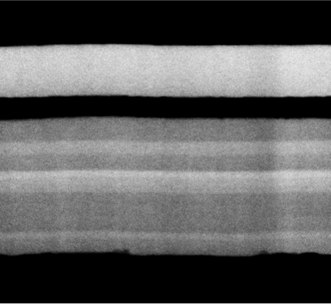
In the alternative approach, a workflow that uses Helios 5 FX keeps the sample in vacuum during the transfer onto the in-chamber scanning or transmission electron microscopy (S/TEM) rod. This prevents degradation due to exposure to air. Performing S/TEM analysis at 30 kV can also be used to highlight the contrast of organic layers (Figure 3).

Figure 3. Using FIB-SEM alone, 30 kV S/TEM can resolve more than 10 layers of an OLED stack.
Enhancing your process metrology workflow
From organic LED to quantum dot to future architectures, advanced process metrology is essential to innovation in display technology. Whether examining a thin-film transistor backplane at micron scale or light-emitting units at nanoscale levels, Thermo Fisher systems provide rapid, efficient and simple solutions that ensure high quality sample preparation and highly repeatable imaging and metrology.
To be continued
This post is the second in our series of four focused on display technology. The next post will cover the failure analysis of backplanes, panels and modules; and our final post will focus on the technology roadmap as it relates to R&D in materials science.
//
Xiaoting Gu is a product marketing manager at Thermo Fisher Scientific
Leave a Reply