Search
_Hero_1440x390_144DPI.jpg)
Materials Science
3D EDS Tomography
3D elemental analysis of materials for nanoscale analysis with chemical and morphological context.
The ability to perform compositional analysis, and visualize the resulting chemical maps in 3D, is essential to obtain the true elemental distribution or composition of a material, ultimately delivering new insights into the structure-function relationship of the sample.
Modern materials research is increasingly reliant on nanoscale analysis in three dimensions. Full 3D characterization includes chemical as well as imaging data, making 3D energy dispersive X-ray spectroscopy (EDS, also abbreviated EDX or XEDS) an indispensable technique. For the highest quality results, instrumentation with dynamic high-resolution imaging capabilities, as well as fast and quantitative data acquisition, is therefore required. The combination of flexibility in acquisition schemes (TEM, STEM, and EDS), the ability to easily and reproducibly optimize the experiment, and the fast and highly sensitive collection of the elemental distribution data are prerequisites for capturing the real 3D structure and composition of nanomaterials.
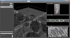
Electron tomography produces 3D reconstructions of materials by incrementally adjusting the angle at which the sample is observed. This produces a tilt series of images that can be digitally back projected to render the original sample volume. EDS spectra can be obtained alongside the the electron microscopy (EM) images, providing detailed elemental context. Below are just a few examples of EDS tomography use cases, covering a wide variety of scales, resolutions, and applications.
Thermo Fisher Scientific instruments offer a range of automation capabilities, allowing you to predetermine mapping conditions, drift compensation, and detector parameters, as well as autofocus and auto tilt conditions. This level of automation enables you to set up the EDS tomography experiment and then leave the system unattended for the complete data acquisition process. Visualization and reconstruction were performed with Thermo Scientific Inspect 3D and Avizo Software.
EDS tomography of P-Zn-In nanotubes, which are used as an electrode material for Na-ion and Li-ion batteries. The segregation of zinc has not been well known during synthesis; however, the elemental data clearly reveals the distribution of zinc relative to the other elements. It becomes evident that there is almost no concentration of zinc in the straight nanotubes. Sample courtesy of Dr. Reza Shahbazian Yassar, Michigan Tech University.

3D EDS TEM tomography of precipitates in an AlMgSi alloy. Sample courtesy of Thomas Kremmer and Stefan Pogatscher, University of Leoben, Austria.
EDS tomography data of organic nanoparticles in a polymer sheet.
EDS tomography data of a catalyst powder. Sample courtesy of Tampere University of Technology, Finland.
EDS tomography data of copper indium sulfide (CuInS2) nanostructures. Sample courtesy of Prof. Neerish Revaprasadu, University of Zululand, South Africa.
Example walkthrough of the EDS tomography workflow on the Talos S/TEM.
STEM and EDS tomography showing the distribution of the Palladium particles (red) relative to other elements of the vehicle aged catalyst material.
Digital slice of the reconstructed Ag-Pt core shell nanoparticle volume. Sample courtesy Prof. Yi Ding and Prof. Jun Luo, Center for Electron Microscopy, Tianjin University of Technology.
Segmented surface rendering of nanoparticles with elements present: Ag core, Platinum shell (to increase visibility, the Platinum shells have been colored semitransparent).
EDS tomography of P-Zn-In nanotubes, which are used as an electrode material for Na-ion and Li-ion batteries. The segregation of zinc has not been well known during synthesis; however, the elemental data clearly reveals the distribution of zinc relative to the other elements. It becomes evident that there is almost no concentration of zinc in the straight nanotubes. Sample courtesy of Dr. Reza Shahbazian Yassar, Michigan Tech University.
3D EDS TEM tomography of precipitates in an AlMgSi alloy. Sample courtesy of Thomas Kremmer and Stefan Pogatscher, University of Leoben, Austria.
EDS tomography data of organic nanoparticles in a polymer sheet.
EDS tomography data of a catalyst powder. Sample courtesy of Tampere University of Technology, Finland.
EDS tomography data of copper indium sulfide (CuInS2) nanostructures. Sample courtesy of Prof. Neerish Revaprasadu, University of Zululand, South Africa.
Example walkthrough of the EDS tomography workflow on the Talos S/TEM.
STEM and EDS tomography showing the distribution of the Palladium particles (red) relative to other elements of the vehicle aged catalyst material.
Digital slice of the reconstructed Ag-Pt core shell nanoparticle volume. Sample courtesy Prof. Yi Ding and Prof. Jun Luo, Center for Electron Microscopy, Tianjin University of Technology.
Segmented surface rendering of nanoparticles with elements present: Ag core, Platinum shell (to increase visibility, the Platinum shells have been colored semitransparent).

Control de proceso
La industria moderna exige un alto rendimiento con una calidad superior, un equilibrio que se mantiene a través de un control de procesos sólido. Las herramientas SEM y TEM con software de automatización exclusivo proporcionan información rápida y multiescala para la supervisión y la mejora de procesos.

Control de calidad
El control y garantía de calidad son esenciales en la industria moderna. Ofrecemos una gama de herramientas de EM y espectroscopía para el análisis multiescala y multimodal de defectos, lo que le permite tomar decisiones fiables e informadas para el control y la mejora de procesos.

Pulcritud
Más que nunca, la fabricación moderna necesita componentes fiables y de calidad. Con la microscopía electrónica de barrido, el análisis de limpieza de las piezas se puede llevar a cabo internamente, lo que le proporciona una amplia gama de datos analíticos y acorta su ciclo de producción.

Investigación sobre materiales fundamentales
Se investigan nuevos materiales a escalas cada vez más pequeñas para lograr el máximo control de sus propiedades físicas y químicas. La microscopía electrónica proporciona a los investigadores información clave sobre una amplia variedad de características materiales a escala nanométrica.

Investigación de baterías
El desarrollo de baterías se realiza mediante análisis multiescala con microCT, SEM y TEM, espectroscopía Raman, XPS y visualización y análisis 3D digital. Aprenda cómo este enfoque proporciona la información estructural y química necesaria para crear mejores baterías.

Investigación sobre polímeros
La microestructura polimérica determina las características y el rendimiento del material a granel. La microscopía electrónica permite un análisis exhaustivo en microescala de la morfología y composición de los polímeros para aplicaciones de control de calidad e I+D.

Investigación sobre metales
La producción eficaz de metales requiere un control preciso de las inclusiones y precipitados. Nuestras herramientas automatizadas pueden realizar varias tareas cruciales para el análisis de metales, incluyendo el recuento de nanopartículas, el análisis químico EDS y la preparación de muestras de TEM.

Nanopartículas
Los materiales tienen propiedades sustancialmente diferentes en la nanoescala y en la macroescala. Para estudiarlos, la instrumentación S/TEM se puede combinar con la espectroscopia de rayos X por dispersión de energía para obtener datos de resolución nanométrica, o incluso subnanométrica.

Gas y petróleo
A medida que la demanda de petróleo y gas continúa, existe la necesidad constante de una extracción eficiente y eficaz de hidrocarburos. Thermo Fisher Scientific ofrece una amplia gama de soluciones de microscopía y espectroscopía para una gran variedad de aplicaciones de la ciencia del petróleo.

Investigación geológica
Las ciencias geológicas están basadas en la observación uniforme y precisa de múltiples escalas de características dentro de las muestras de roca. SEM-EDS, combinado con software de automatización, permite el análisis directo a gran escala de la composición de la textura y los minerales para la investigación de la petrología y la mineralogía.

Investigación sobre catálisis
Los catalizadores son cruciales para la mayoría de los procesos industriales modernos. Su eficacia depende de la composición microscópica y la morfología de las partículas catalíticas; EM con EDS es ideal para estudiar estas propiedades.

Pruebas de materiales para automóviles
Todos los componentes de un vehículo moderno están diseñados para garantizar la máxima seguridad, eficacia y rendimiento. La caracterización detallada de materiales de automoción con microscopía electrónica y espectroscopía informa sobre decisiones cruciales sobre procesos, mejoras de productos y nuevos materiales.

Fibras y filtros
El diámetro, la morfología y la densidad de las fibras sintéticas son parámetros clave que determinan la vida útil y la funcionalidad de un filtro. La microscopía electrónica de barrido (SEM) es la técnica ideal para investigar rápida y fácilmente estas características.
Hoja de estilo para tarjetas originales instrumentos


Style Sheet for Komodo Tabs
Style Sheet to change H2 style to p with em-h2-header class