“Modern semiconductors are becoming more and more complex, so you can’t actually do a full and comprehensive analysis with just one technique,” Senior Application Scientist Paul Mack explains during this Nexsa Surface Analysis System video. “In order to characterize it fully, you need to have multiple techniques.”

The thickness of a high-k material directly impacts semiconductor device performance
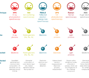
That was the motivation for the Thermo Scientific™ Nexsa XPS system, a powerful tool that combines high-quality XPS with multiple techniques, such as REELS and ISS. Chemical bonding and composition can be measured with the XPS, REELs will provide the band gap information, the ISS provides information from the top monolayer to assess coverage quality, and even Raman is available to provide complimentary information to XPS via the measurement of the chemical’s vibrational structure.
During the video, Paul analyzes the atomic layer deposition (ALD) process of a thin film high-k dielectric material as an example of the Nexsa XPS system’s versatile power. The thickness of the high-k material directly impacts the semiconductor device performance, and the thickness can be measured with XPS. But the Nexsa system adds more value by providing additional techniques: XPS will determine the amount of material deposited, ISS determines whether the layer is a uniform complete film or partial coverage, and REELS measures the band gap of the film as it grows.
Scientists studying semiconductors want repeatable results and precision, and the high sensitivity of the Nexsa XPS system is one of its features that drives that precision, Mack says. “With Nexsa, scientists are going to be able to acquire data much more quickly, with more precision, more reliably, give you higher throughput, and they’re also going to be able to have a much more comprehensive analysis on a single experimental run.”


Leave a Reply