Semiconductor electrical fault isolation
As semiconductor devices and transistor feature dimensions continue to shrink, it’s become increasingly challenging to identify defects that reduce the reliability and performance of the devices that power our everyday consumer and industrial electronics equipment. Smaller devices, high-density interconnects, wafer-level stacking, and complex 3D structures means that more reliability and performance-limiting defects are not found during the chip manufacturing process, leading to an increasing need for electrical fault isolation after devices fail electrical tests at the end of the manufacturing process. Existing solutions have limitations in getting to the exact layer and region of interest. And even if that was possible, there is a significant risk the electron beam used for positioning the probes would influence the transistor performance. Resolving these issues requires precise, site specific delayering and low kV, high resolution SEM imaging.
Nanoprobing
That’s where nanoprobers comes in. Nanoprobers are advanced fault isolation systems that can precisely locate and characterize the nanometer scale electrical faults that impact device performance and reliability. Nanoprobers do this by probing individual transistors and interconnect structures. The availability of precise, site specific delayering capability and damage-free, high resolution SEM nanoprobing has enabled a major inflection point in the fault localization and characterization at advanced technology nodes.

Nanoprobing technology uses probing positioners that can be manipulated and precisely placed on the sample to significantly improve TEM imaging success rates.
TEM failure analysis
TEM failure analysis workflows that don’t incorporate nanoprobing are less efficient in finding the faults that limit device reliability and performance. Nanometer scale faults necessitate the removal of TEM lamella that are 10-30nm thick so the lamella must be placed with nanometer-level accuracy at the exact defect location. If the lamella is not cut in the right place, the TEM will not image the fault and the failure analysis process will need to be repeated on another device. This delays time-to-results and the overall efficiency of the TEM workflow. If the failure analysis is for a customer return on a single device, it would not be possible to repeat the workflow.
By contrast, proper fault isolation with nanoprobing can point to a single transistor and often to a particular section of that transistor, dramatically improving TEM lamella placement and imaging success rates. In fact, incorporating nanoprobing in the TEM can improve the efficiency of the TEM workflow to be as high as 90 percent, several times higher than what is typical if nanoprobing is not utilized.
What does nanoprobe mean?
So how does a nanoprober work? With a scanning electron microscope (SEM) nanoprober, the nanoprobing system is housed within the electron microscope, allowing engineers to manipulate the sample while live imaging at extremely low voltages to avoid sample damage. Users can adjust a set of probing positioners with highly precise movements and see in real time exactly where the tips are positioned. Each probing positioner can be individually controlled and driven to contact the individual transistor elements without damaging the sample. With the most advanced systems, the test results, device parameters, test settings, and images are automatically captured — helping users to accurately identify the smallest defects in the most demanding -cases and improve the efficiency of their failure analysis lab’s workflow.
As yield loss due to non-visible defects continues to rise, advanced nanoprobing technology can help failure analysis laboratories improve their success rates on hard-to-identify defects during the fabrication process. The result is a faster failure analysis workflow that improves production yields and reduces performance problems that can negatively impact a wide range of electronic devices.
For more information on our new nProber IV System, please visit: https://ter.li/nPIV.
John Miller, Ph.D., is a senior product marketing manager for the Nanoprobing Product Line at Thermo Fisher Scientific.
///
Speak with an expert: https://www.thermofisher.com/blog/microscopy/speak-with-an-expert/
Subscribe now to receive Accelerating Microscopy updates straight to your inbox.

Forensic Fractography for Critical Part Failures
How SEM, EBSD, and EDS uncover the microscopic origins of ae... Alice Scarpellini
Read More
Detecting Microscopic Contaminants on Aerospace Production Components
How advanced SEM, EDS, and ToF-SIMS techniques ensure cleanl...
Read More
Lightweight Composite Materials for Aerospace Applications: Strength, Compliance, and Precision Analysis
How multi-scale materials characterization supports safer, l...
Read More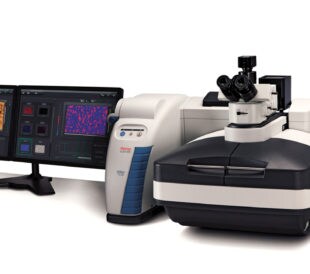
The Essential Guide to Raman Microscopy
What is Raman spectroscopy? With Raman spectroscopy, researc...
Read More
Leave a Reply