 Silicon Drift Detectors (SDDs) are the current state-of-the-art for high resolution, high count rate X-ray spectroscopy. Modern SDDs benefit from a unique design that enables them to achieve a much higher performance than lithium drifted silicon, or Si(Li) detectors. Specifically, they experience far less electronic noise, which is particularly observed at short peaking times (i.e. high count rates), larger detector areas and low X-ray energies. As a result, they have largely displaced Si(Li) detectors and are now used in large quantities for industrial scale applications like scanning electron microscopy/energy dispersive spectroscopy (SEM/EDS) and energy-dispersive X-ray fluorescence (EDXRF), both of which provide faster, more accurate analysis for the mining industry.
SEM/EDS
Since the first SDD-based energy dispersive spectroscopy (EDS) detector was commercially introduced about 15 years ago, X-ray detectors for EDS have undergone a wave of technology enhancements. The first such EDS systems featured an active area of 5 mm2, an energy resolution between 160–200 eV and a maximum collection rate approaching only 100,000 input counts/second. Commercially available SDD-based EDS detectors today feature active areas up to 150 mm2 per device with multiple detectors commonly working in tandem. Collection rates of 1 million input counts/second are an expected standard. Spectral energy resolution down to 121 eV is now available. While energy resolution as measured and reported today is an important metric, it oversimplifies detector performance. (Read The Role of Energy Resolution in Collecting World-Class Data for EDS to learn more.)
EDXRF
The resolution and elemental range achieved by EDXRF analyzers depends on the type of detector used. SDDs have become the most popular detector in EDXRF instrumentation thanks to better resolution, high count rates, and faster results than Si(Li) detectors.
A Typical SDD Device
The figure below shows a typical SDD device. The chip is mounted on a thermoelectric cooler which provides device cooling. SDD devices come in a variety of shapes. The droplet-like shape shown in this figure is commonly used for smaller active areas such as 10 mm2 and 30 mm2. The radiation entrance window which is shown in the picture consists of a flat p-implanted region covered by a thin conductive layer to keep the entrance window radiation hard. ![]()
X-ray Detector Fundamentals
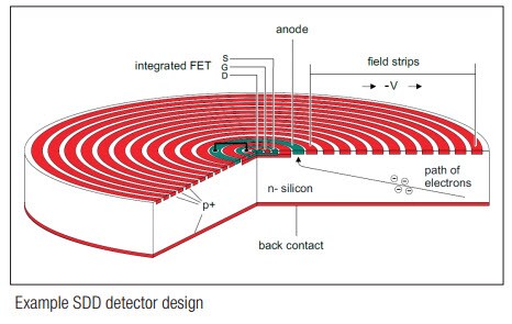
Typical X-ray detection devices consist of an active region composed of fully depleted, high-resistivity silicon, a front contact area and a collection anode. X-rays incident upon the front contact area are absorbed in the bulk Si region and generate electron-hole pairs. The quantity of charged carriers generated depends on the energy of the incident X-ray. A pre-established electric field between the front contact and the anode causes these electrons and holes to drift along the field lines; i.e. toward the anode. The charge accumulated at the anode is then converted to a voltage by a pre-amplifier. The magnitude of this measured voltage corresponds to the energy of the detected X-ray. For an in-depth look at detection technology, including example schematics of the electronics associated with an X-ray detector and SDD detector design, as well as illustrations of voltage steps and associated noise, read the Silicon Drift Detector technical note.


Leave a Reply