Introduction: The quality of transmission electron microscop... Abhi Barve
Read More High-Quality TEM Lamella Preparation: Critical Factors and Best Practices
Removing Large Volumes of Material Fast with FIB-SEMs
Focused ion beam scanning electron microscopes (FIB-SEMs) ar...
Read More Removing Large Volumes of Material Fast with FIB-SEMs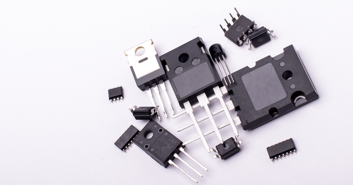
Physical and Electrical Failure Analysis of Power Semiconductor ...
World energy consumption is expected to grow by nearly 50% b... Dr. Adam Stokes
Read More Physical and Electrical Failure Analysis of Power Semiconductor Devices
Accelerating Semiconductor Device Analysis with the Power of the...
Semiconductor fabrication challenges Semiconductor fabricati... Abhi Barve
Read More Accelerating Semiconductor Device Analysis with the Power of the Helios 5 EXL Wafer DualBeam
Unraveling 3D Semiconductor Packaging Challenges
3D semiconductor packaging industry insights from Semicon Ko...
Read More Unraveling 3D Semiconductor Packaging ChallengesNanoscale Microscopy with Gallium FIB SEM
Focused ion beam scanning electron microscopes for precision... Abhi Barve
Read More Nanoscale Microscopy with Gallium FIB SEM
How Advanced Metrology Workflows Solve Critical 3D NAND Structur...
Advanced metrology for 3D NAND structure manufacturing In th... Mark Najarian
Read More How Advanced Metrology Workflows Solve Critical 3D NAND Structure Challenges
New Ablation Solution for Advanced Semiconductor Packaging Incre...
Advanced semiconductor packaging calls for advanced failure ... Dr. Adam Stokes
Read More New Ablation Solution for Advanced Semiconductor Packaging Increases Helios PFIB Throughput and Precision
How 3D Semiconductor Reconstruction with FIB-SEM Reveals Hidden ...
One of the great things about working within the semiconduct... Dr. Adam Stokes
Read More How 3D Semiconductor Reconstruction with FIB-SEM Reveals Hidden Defects and Critical Dimensions
Mapping the Evolving World of Information Display Technology
Display technology has become a constant presence in our liv... Dr. Adam Stokes
Read More Mapping the Evolving World of Information Display Technology