Challenges of non-conductive sample imaging
Electron microscopy has transformed our ability to visualize the world around us, providing nanoscale, if not even atomic-scale, details on everything from metals and polymers to cells and tissues. A fundamental challenge of EM, however, is that it requires samples to be conductive. Without this, the electrons of the beam lack a path to ground, and instead build up on the surface of the specimen. This results in image instability, appearing as bright spots or streaks in the micrograph, causing an overall loss in surface detail and, ultimately, less reliable results. Non-conductive samples can also be more cumbersome to prepare, and the charge effects generally make it more difficult to capture the image and actually see the sample surface, leading to longer imaging sessions and time to data.
Electron microscopy of beam-sensitive and non-conductive material is therefore a pressing concern for researchers, leading to the development of a variety of mitigation strategies, including sample coatings as well as the use of lower voltages and currents. These approaches, unfortunately, come with a variety of drawbacks that make it more challenging to perform analysis, such as coatings potentially obscuring surface details, or poor resolution stemming from reduced beam energies.
Low-vacuum scanning electron microscopy
Low-vacuum mode in scanning electron microscopy (SEM) is a charge-mitigation strategy that allows for the visualization of non-conductive samples without the need for a conductive layer. A relatively higher pressure is maintained in the SEM chamber around the sample through differential pumping, so that the electron column and source remain under high vacuum while the sample is surrounded by a small amount of air and water vapor. These ambient particles keep excess charge from accumulating on the sample surface, thereby enhancing the imaging of non-conductive specimens (see video below).
The Thermo Scientific Axia ChemiSEM System is a scanning electron microscope that offers low-vacuum operation with a single click. It is capable of seamlessly switching between both high and low vacuum modes (up to 150 Pa) and features integrated, live energy-dispersive X-ray spectroscopy (EDS) capability. This allows the Axia ChemiSEM System to provide both secondary and backscattered electron imaging together with EDS elemental characterization for a range of samples, including non-conductive material.
SEM imaging of a non-conductive oxide inclusion in a steel sample. The use of low-vacuum enabled the clear visualization of the inclusion surface with otherwise identical imaging conditions. Inset) Illustration of charge build-up on a non-conductive sample, as well as the mitigative effect of low-vacuum operation in the sample chamber.
Non-conductive inclusion analysis
The analysis of non-conductive regions is often necessary even in otherwise conductive materials. Advanced steels, for instance, can contain a number of beam-sensitive oxide inclusions that researchers may want to characterize; an example of such a particle is shown above. At high-vacuum, the particle accumulates significant charge, concealing structural details. Using the low-vacuum mode of the Axia ChemiSEM System, the secondary electron signal could clearly visualize the structure of the oxide inclusion, at the same imaging conditions, without producing charging artifacts (i.e., at 15 kV, spot size = 4 ~ 0.28 nA, 10 mm WD, 2,500x magnification). This mode was easily enabled through the instrument’s user interface, without the need for additional complex setup or manual adjustment.
Meeting the challenges of non-conductive materials
Low-vacuum SEM expands the scope of non-conductive material analysis that is possible at high voltage and current. In particular, the low-vacuum detector of the Axia ChemiSEM System is specifically designed to efficiently capture secondary electrons, helping to maintain image quality regardless of chamber pressure. This approach facilitates the analysis of not just oxide inclusions, but also ceramics, polymers, coatings, rough or porous surfaces, and many other beam-sensitive materials. With the low-vacuum and live EDS capabilities of the Axia ChemiSEM System, challenging charging artifacts can be quickly transformed into clear, actionable, and reproducible data in just one click.
Watch our on-demand webinar to learn more about the analysis of complex and non-conductive materials
Learn more about the Axia ChemiSEM System

Phenom Desktop SEM for Industrial Quality Control: How Vesuvius Foseco Improved Aluminum Cleanliness Testing
By upgrading their scanning electron microscope (SEM), the V...
Read More
Live SEM EDS Enhances the Microstructure Analysis of Steel
Microstructural analysis of advanced materials There is a ri...
Read More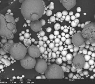
What is scanning electron microscopy?
How does a scanning electron microscope work? You have likel...
Read More
How Does an Electron Microscope Work?
Since the advent of electron microscopy in the 1930s, this r...
Read More
Leave a Reply