Search

Materials Science
Materials Science
Advanced materials characterization with electron microscopy and spectroscopy.
Join the conversation
Advances in materials science
Innovative materials play essential roles in safety, clean energy, transportation, human health, and industrial productivity. To fuel continued innovation, researchers want to deepen their understanding of the physical and chemical properties of materials (morphological, structural, magnetic, thermal, and mechanical) from the macro- to nanoscale. Whether discovering new materials, solving analytical problems, improving processes, or assuring product quality, electron microscopy is capable of providing insight at all scales and modalities. The discoveries resulting from materials science research help enhance researchers’ ability to successfully correlate structural properties with functional performance. In turn, this insight helps commercial enterprises innovate products and processes to gain important time-to-market and cost advantages.
Materials characterization
Analytical solutions, including electron microscopy and spectroscopy, from Thermo Fisher Scientific can help you address your most pressing challenges, including;
- Developing new functional materials that meet the demands of today’s unique social and economic challenges
- Supporting the discovery of new materials with reproducible data from complementary techniques
- Solving materials and method development challenges to improve processes and investigate product defects
- Publishing groundbreaking discoveries, writing winning grant proposals, or patenting novel materials
- Assuring defects are rejected before they reach customers
- Taking your ideas to market quickly and keeping your company competitive
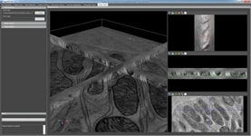
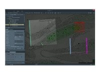
Defect analysis of a lithium ion battery cathode. Serial sectioning and imaging with Plasma FIB DualBeam followed by digital 3D reconstruction using Avizo software provides a highly detailed model of the sample.

Scanning Electron Microscopy for Materials Science
Scanning electron microscopy (SEM) is a powerful imaging technique that uses focused beams of electrons to produce high-resolution, three-dimensional images of sample surfaces at the nanoscale. This method is essential for researchers seeking detailed topographical, compositional, and morphological insights into a wide range of materials.
Industrial manufacturing product selector
The product selector is here to assist you in choosing the most suitable Scanning Electron Microscope (SEM) system and software for your research. Find out in a few minutes which SEM best suits your research application:
Materials Science learning center
Access a targeted collection of application notes, case studies, videos, webinars, and white papers covering a range of applications.

TEM Sample Preparation
Proper sample preparation is a critical step in the scientific experiment process—a step that can determine the ultimate quality and accuracy of the results. FIB-SEM instruments can be used to facilitate fully automated in situ TEM sample preparation, enabling new chemistries and technologies while advancing research in batteries, polymers, metals, and more.
Process control using electron microscopy
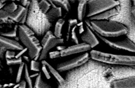
Modern industry demands high throughput with superior quality, a balance that is maintained through robust process control. SEM and TEM tools with dedicated automation software provide rapid, multi-scale information for process monitoring and improvement.
Quality control and failure analysis
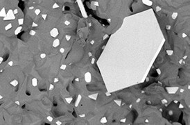
Quality control and assurance are essential in modern industry. We offer a range of EM and spectroscopy tools for multi-scale and multi-modal analysis of defects, allowing you to make reliable and informed decisions for process control and improvement.
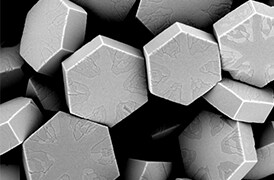
Fundamental Materials Research
Novel materials are investigated at increasingly smaller scales for maximum control of their physical and chemical properties. Electron microscopy provides researchers with key insight into a wide variety of material characteristics at the micro- to nano-scale.
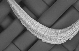
Technical Cleanliness
More than ever, modern manufacturing necessitates reliable, quality components. With scanning electron microscopy, parts cleanliness analysis can be brought inhouse, providing you with a broad range of analytical data and shortening your production cycle.

(S)TEM Sample Preparation
DualBeam microscopes enable the preparation of high-quality, ultra-thin samples for (S)TEM analysis. Thanks to advanced automation, users with any experience level can obtain expert-level results for a wide range of materials.

3D Materials Characterization
Development of materials often requires multi-scale 3D characterization. DualBeam instruments enable serial sectioning of large volumes and subsequent SEM imaging at nanometer scale, which can be processed into high-quality 3D reconstructions of the sample.

Energy Dispersive X-Ray Spectroscopy Elemental Analysis
Energy dispersive X-ray spectroscopy (EDS) techniques provide precise elemental analysis with high speed. Key methods include SEM EDS for integrated imaging and quantification and 3D EDS tomography for detailed nanoscale compositional data. These advancements streamline complex material analyses and enhance research efficiency.

Sample preparation for materials science
We provide comprehensive solutions for sample preparation in materials science, helping ensure precise and reliable results for electron microscopy and other analytical techniques. Our range of instruments allows you to perform cutting, grinding, polishing, and coating of samples, which are crucial steps for achieving high-quality analysis and characterization.

Nanoscale Prototyping
As technology continues to miniaturize, the demand for nanoscale devices and structures is ever increasing. 3D nanoprototyping with DualBeam instruments helps you to quickly design, create, and inspect micro- and nanoscale functional prototypes.
_Technique_800x375_144DPI.jpg)
3D EDS Tomography
Modern materials research is increasingly reliant on nanoscale analysis in three dimensions. 3D characterization, including compositional data for full chemical and structural context, is possible with 3D EM and energy dispersive X-ray spectroscopy.
_Technique_800x375_144DPI.jpg)
EDS Elemental Analysis
Thermo Scientific Phenom Elemental Mapping Software provides fast and reliable information on the distribution of chemical elements within a sample.

Atomic-Scale Elemental Mapping with EDS
Atomic-resolution EDS provides unparalleled chemical context for materials analysis by differentiating the elemental identity of individual atoms. When combined with high-resolution TEM, it is possible to observe the precise organization of atoms in a sample.
_Technique_800x375_144DPI.jpg)
Imaging using HRSTEM and HRTEM
Transmission electron microscopy is invaluable for characterizing the structure of nanoparticles and nanomaterials. High-resolution STEM and TEM enable atomic-resolution data along with information on chemical composition.
_Technique_800x375_144DPI.jpg)
Differential Phase Contrast Imaging
Modern electronics research relies on nanoscale analysis of electric and magnetic properties. Differential phase contrast STEM (DPC-STEM) can image the strength and distribution of magnetic fields in a sample and display the magnetic domain structure.

Imaging Hot Samples
Studying materials in real-world conditions often involves working at high temperatures. The behavior of materials as they recrystallize, melt, deform, or react in the presence of heat can be studied in situ with scanning electron microscopy or DualBeam tools.

Multi-technique surface analysis workflow
To meet the need for extensive characterization of surfaces, we have established multi-technique workflows based on using either the Thermo Scientific ESCALAB CXi XPS Microprobe or the Thermo Scientific Nexsa Surface Analysis System. These instruments are designed as multi-technique workstations to provide comprehensive analyses in a timely and efficient manner.

X-Ray Photoelectron Spectroscopy
X-ray photoelectron spectroscopy (XPS) enables surface analysis, providing elemental composition as well as the chemical and electronic state of the top 10 nm of a material. With depth profiling, XPS analysis extends to compositional insight of layers.
_Technique_800x375_144DPI.jpg)
Environmental SEM (ESEM)
Environmental SEM allows materials to be imaged in their native state. This is ideally suited for academic and industrial researchers who need to test and analyze samples that are wet, dirty, reactive, outgassing or otherwise not vacuum compatible.

Electron Energy Loss Spectroscopy
Materials science research benefits from high-resolution EELS for a wide range of analytical applications. This includes high-throughput, high signal-to-noise-ratio elemental mapping, as well as probing of oxidation states and surface phonons.

APT Sample Preparation
Atom probe tomography (APT) provides atomic-resolution 3D compositional analysis of materials. Focused ion beam (FIB) microscopy is an essential technique for high-quality, orientation, and site-specific sample preparation for APT characterization.

Cross-sectioning
Cross sectioning provides extra insight by revealing sub-surface information. DualBeam instruments feature superior focused ion beam columns for high-quality cross sectioning. With automation, unattended high-throughput processing of samples is possible.

In Situ experimentation
Direct, real-time observation of microstructural changes with electron microscopy is necessary to understand the underlying principles of dynamic processes such as recrystallization, grain growth, and phase transformation during heating, cooling, and wetting.

Particle analysis
Particle analysis plays a vital role in nanomaterials research and quality control. The nanometer-scale resolution and superior imaging of electron microscopy can be combined with specialized software for rapid characterization of powders and particles.

Cathodoluminescence
Cathodoluminescence (CL) describes the emission of light from a material when it is excited by an electron beam. This signal, captured by a specialized CL detector, carries information on the sample’s composition, crystal defects, or photonic properties.

Multi-scale analysis
Novel materials must be analyzed at ever higher resolution while retaining the larger context of the sample. Multi-scale analysis allows for the correlation of various imaging tools and modalities such as X-ray microCT, DualBeam, Laser PFIB, SEM and TEM.

SIMS
The TOF-SIMS (time-of-flight secondary ion mass spectrometry) detector for focused ion beam scanning electron microscopy (FIB-SEM) tools enables high-resolution analytical characterization of all elements in the periodic table, even at low concentrations.

EDS Analysis with ChemiSEM Technology
Energy dispersive X-ray spectroscopy for materials characterization.

The Automated NanoParticle Workflow (APW) is a transmission electron microscope workflow for nanoparticle analysis, offering large area, high resolution imaging and data acquisition at the nanoscale, with on-the-fly processing.

Correlative Imaging and Surface Analysis Workflow
The CISA Workflow’s combination of XPS with SEM analysis enables you to accurately add quantitative chemical composition information of the surface to the structural information from the microscope imagery.

(S)TEM Sample Preparation
DualBeam microscopes enable the preparation of high-quality, ultra-thin samples for (S)TEM analysis. Thanks to advanced automation, users with any experience level can obtain expert-level results for a wide range of materials.

3D Materials Characterization
Development of materials often requires multi-scale 3D characterization. DualBeam instruments enable serial sectioning of large volumes and subsequent SEM imaging at nanometer scale, which can be processed into high-quality 3D reconstructions of the sample.

Energy Dispersive X-Ray Spectroscopy Elemental Analysis
Energy dispersive X-ray spectroscopy (EDS) techniques provide precise elemental analysis with high speed. Key methods include SEM EDS for integrated imaging and quantification and 3D EDS tomography for detailed nanoscale compositional data. These advancements streamline complex material analyses and enhance research efficiency.

Sample preparation for materials science
We provide comprehensive solutions for sample preparation in materials science, helping ensure precise and reliable results for electron microscopy and other analytical techniques. Our range of instruments allows you to perform cutting, grinding, polishing, and coating of samples, which are crucial steps for achieving high-quality analysis and characterization.

Nanoscale Prototyping
As technology continues to miniaturize, the demand for nanoscale devices and structures is ever increasing. 3D nanoprototyping with DualBeam instruments helps you to quickly design, create, and inspect micro- and nanoscale functional prototypes.
_Technique_800x375_144DPI.jpg)
3D EDS Tomography
Modern materials research is increasingly reliant on nanoscale analysis in three dimensions. 3D characterization, including compositional data for full chemical and structural context, is possible with 3D EM and energy dispersive X-ray spectroscopy.
_Technique_800x375_144DPI.jpg)
EDS Elemental Analysis
Thermo Scientific Phenom Elemental Mapping Software provides fast and reliable information on the distribution of chemical elements within a sample.

Atomic-Scale Elemental Mapping with EDS
Atomic-resolution EDS provides unparalleled chemical context for materials analysis by differentiating the elemental identity of individual atoms. When combined with high-resolution TEM, it is possible to observe the precise organization of atoms in a sample.
_Technique_800x375_144DPI.jpg)
Imaging using HRSTEM and HRTEM
Transmission electron microscopy is invaluable for characterizing the structure of nanoparticles and nanomaterials. High-resolution STEM and TEM enable atomic-resolution data along with information on chemical composition.
_Technique_800x375_144DPI.jpg)
Differential Phase Contrast Imaging
Modern electronics research relies on nanoscale analysis of electric and magnetic properties. Differential phase contrast STEM (DPC-STEM) can image the strength and distribution of magnetic fields in a sample and display the magnetic domain structure.

Imaging Hot Samples
Studying materials in real-world conditions often involves working at high temperatures. The behavior of materials as they recrystallize, melt, deform, or react in the presence of heat can be studied in situ with scanning electron microscopy or DualBeam tools.

Multi-technique surface analysis workflow
To meet the need for extensive characterization of surfaces, we have established multi-technique workflows based on using either the Thermo Scientific ESCALAB CXi XPS Microprobe or the Thermo Scientific Nexsa Surface Analysis System. These instruments are designed as multi-technique workstations to provide comprehensive analyses in a timely and efficient manner.

X-Ray Photoelectron Spectroscopy
X-ray photoelectron spectroscopy (XPS) enables surface analysis, providing elemental composition as well as the chemical and electronic state of the top 10 nm of a material. With depth profiling, XPS analysis extends to compositional insight of layers.
_Technique_800x375_144DPI.jpg)
Environmental SEM (ESEM)
Environmental SEM allows materials to be imaged in their native state. This is ideally suited for academic and industrial researchers who need to test and analyze samples that are wet, dirty, reactive, outgassing or otherwise not vacuum compatible.

Electron Energy Loss Spectroscopy
Materials science research benefits from high-resolution EELS for a wide range of analytical applications. This includes high-throughput, high signal-to-noise-ratio elemental mapping, as well as probing of oxidation states and surface phonons.

APT Sample Preparation
Atom probe tomography (APT) provides atomic-resolution 3D compositional analysis of materials. Focused ion beam (FIB) microscopy is an essential technique for high-quality, orientation, and site-specific sample preparation for APT characterization.

Cross-sectioning
Cross sectioning provides extra insight by revealing sub-surface information. DualBeam instruments feature superior focused ion beam columns for high-quality cross sectioning. With automation, unattended high-throughput processing of samples is possible.

In Situ experimentation
Direct, real-time observation of microstructural changes with electron microscopy is necessary to understand the underlying principles of dynamic processes such as recrystallization, grain growth, and phase transformation during heating, cooling, and wetting.

Particle analysis
Particle analysis plays a vital role in nanomaterials research and quality control. The nanometer-scale resolution and superior imaging of electron microscopy can be combined with specialized software for rapid characterization of powders and particles.

Cathodoluminescence
Cathodoluminescence (CL) describes the emission of light from a material when it is excited by an electron beam. This signal, captured by a specialized CL detector, carries information on the sample’s composition, crystal defects, or photonic properties.

Multi-scale analysis
Novel materials must be analyzed at ever higher resolution while retaining the larger context of the sample. Multi-scale analysis allows for the correlation of various imaging tools and modalities such as X-ray microCT, DualBeam, Laser PFIB, SEM and TEM.

SIMS
The TOF-SIMS (time-of-flight secondary ion mass spectrometry) detector for focused ion beam scanning electron microscopy (FIB-SEM) tools enables high-resolution analytical characterization of all elements in the periodic table, even at low concentrations.

EDS Analysis with ChemiSEM Technology
Energy dispersive X-ray spectroscopy for materials characterization.

The Automated NanoParticle Workflow (APW) is a transmission electron microscope workflow for nanoparticle analysis, offering large area, high resolution imaging and data acquisition at the nanoscale, with on-the-fly processing.

Correlative Imaging and Surface Analysis Workflow
The CISA Workflow’s combination of XPS with SEM analysis enables you to accurately add quantitative chemical composition information of the surface to the structural information from the microscope imagery.

Battery Research
Battery development is enabled by multi-scale analysis with microCT, SEM and TEM, Raman spectroscopy, XPS, and digital 3D visualization and analysis. Learn how this approach provides the structural and chemical information needed to build better batteries.

Metals Research and Characterization
Effective production of metals requires precise control of inclusions and precipitates. Our automated tools can perform a variety of tasks critical for metal analysis including; nanoparticle counting, EDS chemical analysis and TEM sample preparation.

Polymers Research
Polymer microstructure dictates the material’s bulk characteristics and performance. Electron microscopy enables comprehensive microscale analysis of polymer morphology and composition for R&D and quality control applications.

Geological Research
Geoscience relies on consistent and accurate multi-scale observation of features within rock samples. SEM-EDS, combined with automation software, enables direct, large-scale analysis of texture and mineral composition for petrology and mineralogy research.

Oil and Gas
As the demand for oil and gas continues, there is an ongoing need for efficient and effective extraction of hydrocarbons. Thermo Fisher Scientific offers a range of microscopy and spectroscopy solutions for a variety of petroleum science applications.

Nanoparticles
Materials have fundamentally different properties at the nanoscale than at the macroscale. To study them, S/TEM instrumentation can be combined with energy dispersive X-ray spectroscopy to obtain nanometer, or even sub-nanometer, resolution data.

Forensics
Micro-traces of crime scene evidence can be analyzed and compared using electron microscopy as part of a forensic investigation. Compatible samples include glass and paint fragments, tool marks, drugs, explosives, and GSR (gunshot residue).

Catalysis Research
Catalysts are critical for a majority of modern industrial processes. Their efficiency depends on the microscopic composition and morphology of the catalytic particles; EM with EDS is ideally suited for studying these properties.

Fibers and Filters
The diameter, morphology and density of synthetic fibers are key parameters that determine the lifetime and functionality of a filter. Scanning electron microscopy (SEM) is the ideal technique for quickly and easily investigating these features.

2D Materials
Novel materials research is increasingly interested in the structure of low-dimensional materials. Scanning transmission electron microscopy with probe correction and monochromation allows for high-resolution two-dimensional materials imaging.

Automotive Materials Testing
Every component in a modern vehicle is designed for safety, efficiency, and performance. Detailed characterization of automotive materials with electron microscopy and spectroscopy informs critical process decisions, product improvements, and new materials.

Food Development and Testing
To ensure food safety, protect your brand, and ensure consumer satisfaction, analytical testing and material characterization instruments avert costly errors and product defects and help you deliver consistently delicious foods and beverages.
Electron microscopy services for
the materials science
To ensure optimal system performance, we provide you access to a world-class network of field service experts, technical support, and certified spare parts.


