Additive manufacturing (AM) is revolutionizing how materials are built. Constructing objects by adding successive super-fine layers of material, manufacturers can avoid areas of weakness such as surfaces that are mechanically welded together. The result is stronger and lighter components, and the ability to form complex designs that would otherwise be too expensive to build.
Additive manufacturing challenges
As materials scientists optimize their AM methods, they are discovering that additive manufacturing techniques provide new challenges in determining what materials processing steps result in the target material properties. Quantifying these challenges requires advanced multi-scale, multi-modal characterization approaches to properly relate observed defects to material performance. Researchers are working to discover failures at the micro-level—and doing so requires correlating and analyzing data collected from various X-ray and electron microscopy techniques. By examining their cumulative data, researchers can determine microscopic failures that undermine the strength of the finished component. Yet completing this work manually can be labor-intensive and prone to error.
Correlative microscopy for multi-scale multi-modal analysis
The good news is that Thermo Scientific Maps Software helps tackle this challenge. Maps Software provides an intuitive platform for bringing together all the images collected from a sample in one place, making it easier for researchers to obtain a full picture of components built using additive manufacturing methods.
Take Inconel 718, a nickel-based alloy used for turbine components. To avoid failures, it’s critical that this component be built to resist pressure and corrosion, and to withstand temperatures up to 1300 degrees Fahrenheit. Using Maps to check the quality of Inconel 718 turbine components developed using additive manufacturing, researchers can easily combine multiple types of data at different scales to obtain the complete information they need.
A quality check of an AM developed part typically involves several steps. A critical first step is to examine the entire sample using micro-computed tomography (microCT), like our HeliScan microCT, to have an internal view of the sample, identify and defects and determine what additional characterization steps are needed. In the case of investigating fractures, researchers will be interested in the microstructure, where fractures are forming and what is causing them to propagate. In the Inconel example, after 3D imaging in the MicroCT, the sample was subjected to a workflow that included optical microscopy, scanning electron microscopy, and targeted, high resolution 3D analysis using a Focused Plasma Ion Beam SEM (PFIB-SEM).
In addition to characterization using basic imaging, electron microscopy provides several useful signals to investigate the composition and structure of a material. In this example, Electron Backscattered Diffraction (EBSD)-a technique to quantify the crystallographic orientations of materials-was used to interpret the microstructure and investigate strain around fractures. When deploying multi-scale, multi-modal workflows, there are so many approaches, so much data to keep track of, and areas of interest to target it can become difficult to know where to start, or what areas will be the best target for analysis. So how can you approach obtaining this data intelligently?

A fracture within a parts component shown at two scales using Maps Software. Maps Software makes it easy to align and correlate data among different images so information can be examined at different scales.
Benefits of correlative microscopy for additive manufacturing
The beauty of Maps Software is that it helps to simplify the analysis of data from all these different techniques. Using Maps Software, the researchers can automatically set up the system to acquire high-resolution images in areas of interest. They can then correlate all the images and data, quickly zooming in and out and moving between images to examine the sample at different scales. Each layer of information can be turned on or off, making it easy to hone in on specific information. What’s more, the researchers can analyze their data anytime, anywhere from their laptop, giving them full flexibility to collaborate with colleagues and review their results.
Using Maps to examine all their images and data in one place, researchers can quickly check the nature of the microstructure of the Inconel 718 turbine component, over a range of build conditions. They can then use this information to make changes to the additive manufacturing process, ensuring the right parameters are applied to produce a part with the target material properties.
As additive manufacturing continues to advance, it’s important to equip researchers with the robust tools they need to perfect their production processes and avoid material failures. Maps software addresses this challenge, helping to optimize the next generation of manufactured products.
Eric Goergen is a product marketing manager in the Analytical Instrument Group at Thermo Fisher Scientific.
///
To read more on how Maps Software transforms data analysis for materials scientists, please click here.
Subscribe now to receive Accelerating Microscopy updates straight to your inbox.
Speak with an expert: https://www.thermofisher.com/blog/microscopy/speak-with-an-expert/

Lightweight Composite Materials for Aerospace Applications: Strength, Compliance, and Precision Analysis
How multi-scale materials characterization supports safer, l...
Read More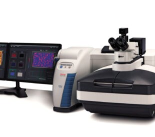
The Essential Guide to Raman Microscopy
What is Raman spectroscopy? With Raman spectroscopy, researc...
Read More
Particle Analysis for Micro Machining
With the need for small, precisely crafted parts in products...
Read More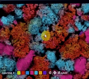
You Need an Efficient and Intuitive SEM Experience
Researchers at today’s industrial labs typically work unde...
Read More
Leave a Reply