Search
Focused ion beam scanning electron microscopy
FIB-SEM Instruments
Scientists and engineers in both academia and industry are constantly facing new challenges that require highly localized characterization of a wide range of samples and materials. The ongoing drive to improve the quality of these materials means that structural and compositional information at the nanoscale is frequently necessary. FIB-SEM instruments generate exactly this kind of data by combining the precise sample modification of FIB with the high-resolution imaging of SEM.
DualBeam instruments
Thermo Fisher Scientific is the industry leader in FIB-SEM technology with more than 30 years of experience with DualBeams. The technology's novel ability to reveal subsurface structural detail, by making precise cuts with a FIB and then imaging the exposed surface with a high-resolution SEM, has led to its acceptance by researchers and engineers in a wide variety of applications. With more than 2,000 Thermo Scientific systems installed around the world, our DualBeams continue to lead the market with cutting-edge capabilities built on technical innovation and a deep store of application knowledge gathered over years of collaborative development with our customers.
TriBeam instruments
The new TriBeam systems are our latest FIB-SEM innovation, featuring the addition of a femtosecond laser, which can cut many materials at rates that are orders of magnitude faster than a typical FIB. A large cross-section (hundreds of micrometers) can be created in less than five minutes. Because the laser has a different removal mechanism (ablation versus the ion sputtering of FIB), it can easily process challenging materials, such as non-conductive or ion-beam-sensitive samples. The extremely short duration of the femtosecond laser pulses introduces almost no artifacts such as heat impact, microcracking, melting, or those typical of traditional mechanical polishing. In most cases, the laser-milled surfaces are clean enough for direct SEM imaging and even for surface-sensitive techniques such as electron backscatter diffraction (EBSD) mapping.
We offer a broad product portfolio and advanced automation capabilities for applications such as transmission electron microscopy (TEM) sample preparation, subsurface and 3D characterization, nano-prototyping, and in situ experimentation.
Style Sheet for Fonts
Style Sheet for Instrument Cards Original
TEM sample preparation
TEM sample preparation is considered to be one of the most critical tasks in materials science research. However, it is also one of the most challenging and time-consuming. The latest technological innovations of DualBeam technology, along with our comprehensive software solutions and application expertise, enable fast and easy preparation of site-specific, high-quality S/TEM (scanning/transmission electron microscopy) samples for a wide range of materials. Thermo Scientific AutoTEM Software adds the capability for fully automated, unattended in situ TEM sample preparation, significantly increasing throughput and bringing you expert-level results regardless of your experience. Learn more about TEM sample prep.
3D Structural analysis
When combined with Thermo Scientific Auto Slice & View Software, DualBeam instruments provide 3D insight into sample structure by selectively removing (milling) the material for subsurface characterization. Digital reconstruction generates multi-modal 3D datasets that can consist of a variety of signals, including backscattered electron (BSE) imaging for maximum materials contrast, energy dispersive spectroscopy (EDS) for compositional information, and electron backscatter diffraction (EBSD) for microstructural and crystallographic information.
The SEM capability of DualBeam instruments offers nanoscale details across a wide range of working conditions, from structural information obtained at 30 keV in STEM mode to charge-free, detailed surface information at lower energies. With unique in-lens detectors, DualBeam systems are designed for simultaneous acquisition of angular/energy-selective secondary-electron and BSE data. Fast, accurate, and reproducible results are provided by our unique SEM column design, which features fully automated lens alignments.
Large-volume, millimeter-scale characterization
Thermo Scientific TriBeam systems are (plasma) FIB-SEM instruments combined with a femtosecond laser for ultrafast material removal and millimeter-scale 3D characterization with nanometer resolution. Learn more about TriBeam instruments.
Nanoprototyping
As technology continues to miniaturize, the demand for nanoscale devices and structures is ever increasing. The challenge of converting the latest ideas and designs into valuable assets only continues to grow, and significant technical and financial barriers need to be overcome for successful prototyping of nanoscale devices.
Standard nanofabrication batch processes involve the combined use of different machines for each pattern layer. These instruments might include a spin coater for resist application, a lithography tool, wet chemistry for resist development, a plasma cleaner, and deposition or etching equipment for pattern transfer. The use of so many distinct tools results in a costly and time-consuming prototyping process. As researchers push nanotechnology towards smaller dimensions, these established procedures and recipes often no longer keep pace with the demands of rapid development.
Thermo Fisher Scientific offers a smart and efficient way of turning nanoscale designs into reality. The nanopatterning capabilities of our FIB-SEM systems can substantially reduce research and development time. Rapid prototyping with the FIB enables functionality testing before the final device layout is established for batch fabrication. Beam-induced deposition of different materials can be combined with FIB milling without the need for additional aligning lithography steps; patterns can be directly added to deposited structures or existing patterns can be modified. The final patterned substrates are immediately available for further processing or characterization. Together, these produce a robust prototyping workflow that enables you to quickly design, create, and inspect micro- and nanoscale functional prototype devices.


Nanoscale Materials Characterization
Understanding the nanoscale characteristics of materials is the first step in creating the next generation of lighter, stronger, and more energy efficient solutions. With our electron microscopy solutions, we help you simplify this complex material journey and accelerate your nanoscale materials research. Nanoscale workflow is a journey of material from bulk to nanometer scales using our DualBeam FIB-SEM for sample preparation and Transmission Electron Microscopes for material analysis.

Electron microscopy learning center
Electron microscopy resources and reference materials for microscopy novices, experts, and everyone in between. The electron microscopy learning center provides a variety of informational and educational resources on electron microscopy for students, educators, or anyone that simply wants to learn more about this fascinating technology.
Style Sheet to change H2 style to p with em-h2-header class

TEM sample of a nickel super alloy material being prepared by FIB milling. This SEM image shows the initial chunking step, which consists of a high-current rough cut followed by a medium-current polish.

SEM image of a nickel super alloy sample attached to a grid after lift-out.

High-resolution STEM image of an ultra-thin TEM lamella, which shows the arrangement of individual atomic columns of strontium titanate. Sample prepared with the Helios DualBeam.

Aluminum sample where a 5x6 array of STEM lamella has been prepared in 6 hours with AutoTEM Software, undercut and ready for lift-out during fully automated, unattended operation.

Automated drift-corrected nano-pillar milling produced with multiple beam currents and Autoscript Software. Horizontal field width = 10 µm.

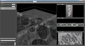
3D quantitative analysis of Li-ion battery graphite anode. The data has been acquired using a Thermo Scientific Helios 5 Laser PFIB System, followed by reconstruction and visualization with Thermo Scientific Avizo Software.
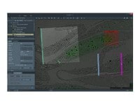
3D reconstruction of an automotive oil filter casing, acquired with the Helios Hydra DualBeam and Auto Slice & View 4 Software for automated serial sectioning. Horizontal field width = 350 µm.
Documents
TEM sample of a nickel super alloy material being prepared by FIB milling. This SEM image shows the initial chunking step, which consists of a high-current rough cut followed by a medium-current polish.
SEM image of a nickel super alloy sample attached to a grid after lift-out.
High-resolution STEM image of an ultra-thin TEM lamella, which shows the arrangement of individual atomic columns of strontium titanate. Sample prepared with the Helios DualBeam.
Aluminum sample where a 5x6 array of STEM lamella has been prepared in 6 hours with AutoTEM Software, undercut and ready for lift-out during fully automated, unattended operation.
Automated drift-corrected nano-pillar milling produced with multiple beam currents and Autoscript Software. Horizontal field width = 10 µm.
3D quantitative analysis of Li-ion battery graphite anode. The data has been acquired using a Thermo Scientific Helios 5 Laser PFIB System, followed by reconstruction and visualization with Thermo Scientific Avizo Software.
3D reconstruction of an automotive oil filter casing, acquired with the Helios Hydra DualBeam and Auto Slice & View 4 Software for automated serial sectioning. Horizontal field width = 350 µm.
Documents
Style Sheet for Komodo Tabs
Electron microscopy services
To ensure optimal system performance, we provide you access to a world-class network of field service experts, technical support, and certified spare parts.