Seeking enhanced performance with compound semiconductor waf...
Read More Using Electron Channeling Contrast Imaging to Optimize Defect Analysis and Wafer Fabrication
Semiconductor manufacturing stories and solutions about a more connected, more autonomous, and smarter world
Seeking enhanced performance with compound semiconductor waf...
Read More Using Electron Channeling Contrast Imaging to Optimize Defect Analysis and Wafer Fabrication
For decades, the semiconductor industry has been defined by ...
Read More Advanced Semiconductor Packaging: Bringing Stacked Chips Together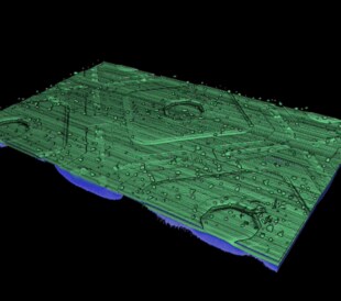
3D semiconductor reconstruction to address industry challeng...
Read More The Value of 3D Semiconductor Reconstruction for Identifying Defects and Measuring Critical Dimensions
Semiconductor process development Accelerating product devel...
Read More Semiconductor Advancement and Time-To-Market Enhanced with New Circuit Edit Solution
The first three blogs in this series focused on present-day ...
Read More How to Clear R&D Hurdles in Display Technology Engineering
Display technology relies on a complex, multi-stage manufact...
Read More How to Improve Quality and Yield with Early Failure Analysis of Semiconductor Devices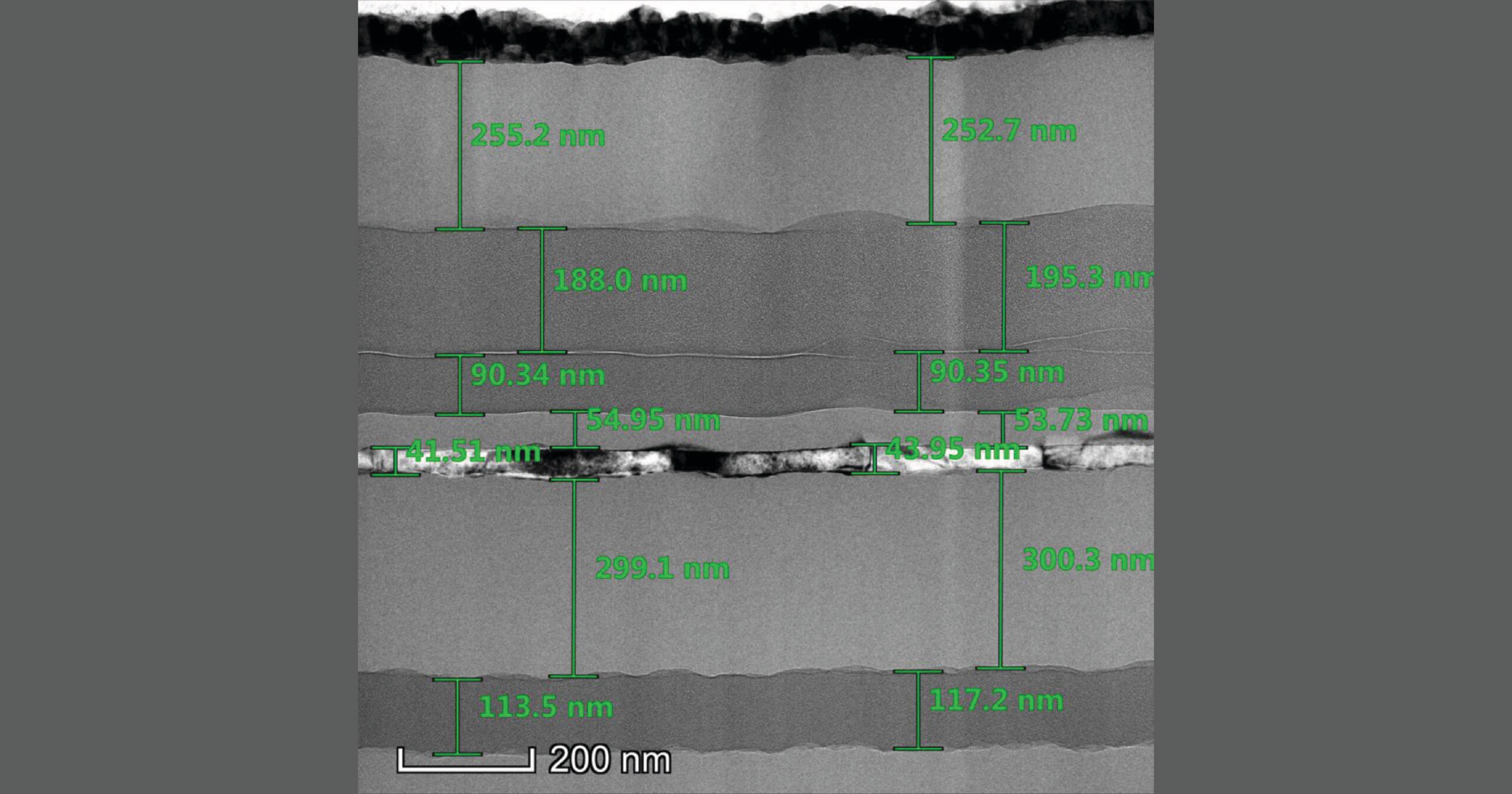
Process metrology and the development of display technology ...
Read More How Advanced Process Metrology Enables Crucial Layer Examination of Display Technology
Semiconductors have changed the world. Though brief, in the ...
Read More A History of Semiconductor Engineering and Electron Microscopy, 40 Years Young
Display technology has become a constant presence in our liv...
Read More Mapping the Evolving World of Information Display Technology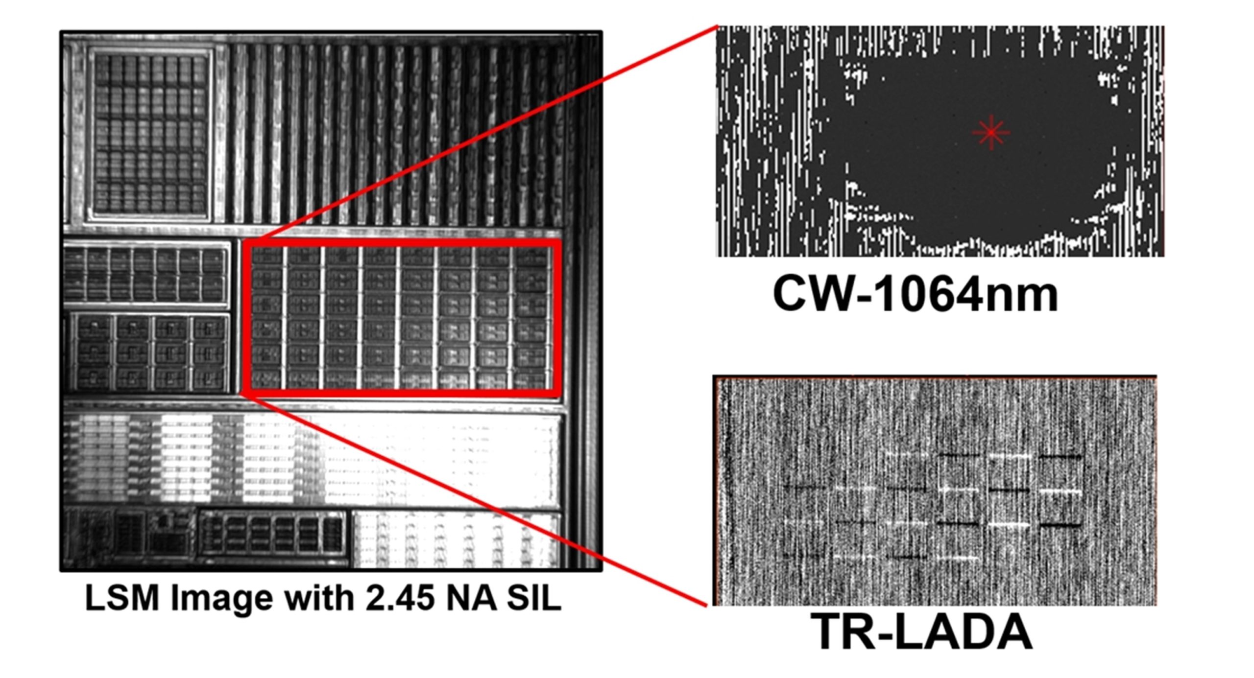
Three challenges seem to be ever-present in the semiconducto...
Read More Enhancing Semiconductor Fault Isolation With Time-resolved Laser-assisted Device Alteration